


The Shape of Molecules

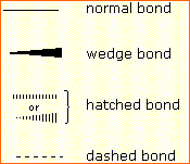 In order to represent such configurations on a two-dimensional surface (paper, blackboard or screen), we often use perspective drawings in which the direction of a bond is specified by the line connecting the bonded atoms. In
most cases the focus of configuration is a carbon atom so the lines
specifying bond directions will originate there. As defined in the
diagram on the right, a simple straight line represents a bond lying
approximately in the surface plane. The two bonds to substituents A
in the structure on the left are of this kind. A wedge shaped bond is
directed in front of this plane (thick end toward the viewer), as shown
by the bond to substituent B; and a hatched bond is directed in back of the plane (away from the viewer), as shown by the bond to substituent D.
Some texts and other sources may use a dashed bond in the same manner
as we have defined the hatched bond, but this can be confusing because
the dashed bond is often used to represent a partial bond (i.e. a
covalent bond that is partially formed or partially broken). The
following examples make use of this notation, and also illustrate the
importance of including non-bonding valence shell electron pairs
(colored blue) when viewing such configurations .
In order to represent such configurations on a two-dimensional surface (paper, blackboard or screen), we often use perspective drawings in which the direction of a bond is specified by the line connecting the bonded atoms. In
most cases the focus of configuration is a carbon atom so the lines
specifying bond directions will originate there. As defined in the
diagram on the right, a simple straight line represents a bond lying
approximately in the surface plane. The two bonds to substituents A
in the structure on the left are of this kind. A wedge shaped bond is
directed in front of this plane (thick end toward the viewer), as shown
by the bond to substituent B; and a hatched bond is directed in back of the plane (away from the viewer), as shown by the bond to substituent D.
Some texts and other sources may use a dashed bond in the same manner
as we have defined the hatched bond, but this can be confusing because
the dashed bond is often used to represent a partial bond (i.e. a
covalent bond that is partially formed or partially broken). The
following examples make use of this notation, and also illustrate the
importance of including non-bonding valence shell electron pairs
(colored blue) when viewing such configurations .
Bonding configurations are readily predicted by valence-shell electron-pair repulsion theory, commonly referred to as VSEPR in most introductory chemistry texts. This simple model is based on the fact that electrons repel each other, and that it is reasonable to expect that the bonds and non-bonding valence electron pairs associated with a given atom will prefer to be as far apart as possible. The bonding configurations of carbon are easy to remember, since there are only three categories.

In the three examples shown above, the central atom (carbon) does not have any non-bonding valence electrons; consequently the configuration may be estimated from the number of bonding partners alone. For molecules of water and ammonia, however, the non-bonding electrons must be included in the calculation. In each case there are four regions of electron density associated with the valence shell so that a tetrahedral bond angle is expected. The measured bond angles of these compounds (H2O 104.5º & NH3 107.3º) show that they are closer to being tetrahedral than trigonal or linear. Of course, it is the configuration of atoms (not electrons) that defines the the shape of a molecule, and in this sense ammonia is said to be pyramidal (not tetrahedral). The compound boron trifluoride, BF3, does not have non-bonding valence electrons and the configuration of its atoms is trigonal. Nice treatments of VSEPR theory have been provided by Oxford and Purdue . Click on the university name to visit their site.
The best way to study the three-dimensional shapes of molecules is by
using molecular models. Many kinds of model kits are available to
students and professional chemists. Some of the useful features of
physical models can be approximated by the model viewing applet Jmol.
This powerful visualization tool allows the user to move a molecular
stucture in any way desired. Atom distances and angles are easily
determined. To measure a distance, double-click on two atoms. To measure
a bond angle, do a double-click, single-click, double-click on three
atoms. To measure a torsion angle, do a double-click, single-click,
single-click, double-click on four atoms. A pop-up menu of commands may
be accessed by the right button on a PC or a control-click on a Mac
while the cursor is inside the display frame.
You may examine several Jmol models of compounds discussed above by
.
One way in which the shapes of molecules manifest themselves experimentally is through molecular dipole moments. A molecule which has one or more polar covalent bonds may have a dipole moment as a result of the accumulated bond dipoles. In the case of water, we know that the O-H covalent bond is polar, due to the different electronegativities of hydrogen and oxygen. Since there are two O-H bonds in water, their bond dipoles will interact and may result in a molecular dipole which can be measured. The following diagram shows four possible orientations of the O-H bonds.

The bond dipoles are colored magenta and the resulting molecular dipole is colored blue. In the linear configuration (bond angle 180º) the bond dipoles cancel, and the molecular dipole is zero. For other bond angles (120 to 90º) the molecular dipole would vary in size, being largest for the 90º configuration. In a similar manner the configurations of methane (CH4) and carbon dioxide (CO2) may be deduced from their zero molecular dipole moments. Since the bond dipoles have canceled, the configurations of these molecules must be tetrahedral (or square-planar) and linear respectively.
The case of methane provides insight to other arguments that have been
used to confirm its tetrahedral configuration. For purposes of
discussion we shall consider three other configurations for CH4, square-planar, square-pyramidal and triangular-pyramidal.
Models of these possibilities may be examined by
.
Substitution of one hydrogen by a chlorine atom gives a CH3Cl compound. Since the tetrahedral, square-planar and square-pyramidal configurations have structurally equivalent hydrogen atoms, they would each give a single substitution product. However, in the trigonal-pyramidal configuration one hydrogen (the apex) is structurally different from the other three (the pyramid base). Substitution in this case should give two different CH3Cl compounds if all the hydrogens react. In the case of disubstitution, the tetrahedral configuration of methane would lead to a single CH2Cl2 product, but the other configurations would give two different CH2Cl2 compounds. These substitution possibilities are shown in the above insert.
Isomers |
|---|
Isomers
Structural Formulas
It is necessary to draw structural formulas for organic compounds
because in most cases a molecular formula does not uniquely represent a
single compound. Different compounds having the same molecular formula
are called isomers, and the prevalence of organic isomers
reflects the extraordinary versatility of carbon in forming strong
bonds to itself and to other elements.
When the group of atoms that
make up the molecules of different isomers are bonded together in
fundamentally different ways, we refer to such compounds as constitutional isomers. There are seven constitutional isomers of C4H10O, and structural formulas for these are drawn in the following table. These formulas represent all known and possible C4H10O compounds, and display a common structural feature. There are no double or triple bonds and no rings in any of these structures.. Note that each of the carbon atoms is bonded to four other atoms, and is saturated with bonding partners.

Developing the ability to visualize a three-dimensional structure from two-dimensional formulas requires practice, and in most cases the aid of molecular models. As noted earlier, many kinds of model kits are available to students and professional chemists, and the beginning student is encouraged to obtain one.
Constitutional isomers have the same molecular formula, but their physical and chemical properties may be very different.
For an example Click Here.
Distinguishing Carbon Atoms: When discussing structural formulas, it is often useful to distinguish different groups of carbon atoms by their structural characteristics. A primary carbon (1º) is one that is bonded to no more than one other carbon atom. A secondary carbon (2º) is bonded to two other carbon atoms, and tertiary (3º) and quaternary (4º) carbon atoms are bonded respectively to three and four other carbons. The three C5H12 isomers shown below illustrate these terms.

Structural differences may occur within these four groups, depending on the molecular constitution. In the formula on the right all four 1º-carbons are structurally equivalent (remember the tetrahedral configuration of tetravalent carbon); however the central formula has two equivalent 1º-carbons (bonded to the 3º carbon on the left end) and a single, structurally different 1º-carbon (bonded to the 2º-carbon) at the right end. Similarly, the left-most formula has two structurally equivalent 2º-carbons (next to the ends of the chain), and a structurally different 2º-carbon in the middle of the chain. A consideration of molecular symmetry helps to distinguish structurally equivalent from nonequivalent atoms and groups. The ability to distinguish structural differences of this kind is an essential part of mastering organic chemistry. It will come with pr
actice and experience.
Some Evidence for Molecular Structure
One of the most remarkable achievements of modern chemistry is the capability to draw accurate structural formulas for complex molecules. Considering that molecules are much too small to be seen by even the strongest optical microscopes, how is it that the connectivity and relative location of the component atoms can be assigned with confidence?
Prior to 1950, molecular structures were deduced largely
by chemical degradation of large complex molecules into smaller known
fragments. The terpene hydrocarbon myrcene provides a simple example, as
shown in the following diagram.

Combustion analysis yielded the ratio of carbon to hydrogen by measuring the amount of carbon dioxide and water produced, and a rough molecular weight was obtained from boiling point studies. The double bond functional groups were assayed by catalytic hydrogenation, and cleavage by ozonolysis yielded the known small molecules formaldehyde and acetone. Further oxidation formed succinic acid with the loss of carbon dioxide. The logical assembly of these fragments into the struture of myrcene, essentially a chemical jigsaw puzzle, required perseverance and the insight of experience on the part of early chemists.
If
this were the present status of structure determination, knowledge of
the characteristic reactivity of the common functional groups, and the
nuances of their interactions with each other would be a minimal
requirement for achieving a basic understanding of this field. Over the
past fifty years, however, a more easily applied and interpreted set of
tools for this purpose has been developed and are now widely used by
chemists for the elucidation of molecular structures.
Most of what
we know about the structure of atoms and molecules comes from studying
their interaction with light (electromagnetic radiation), a subject
called spectroscopy, and a full introduction to spectroscopy
will be found elsewhere in this text. Fortunately, spectroscopic
applications to molecular structure are sufficiently straightforward
that they can be appreciated without delving into the exact nature of
the methods. In the following discussion, information provided by three
different spectroscopic tools will be described.
(i) Mass Spectrometry: This provides a molecular weight measurement accurate to less than 0.1 Da (atomic mass units) .
(ii) 13C Nuclear Magnetic Resonance Spectroscopy: This detects structurally different carbon atoms within a molecule.
(iii) Infrared Spectroscopy: This detects and identifies functional groups within a molecule.

To begin, consider the three isomeric C5H12 alkanes, molecular weight = 72. These are all low boiling liquids lacking reactive functional groups. Despite their similarity, they are easily distinguished by the number of structurally distinct carbon atoms in each, as disclosed by 13C nmr. In the following diagram equivalent carbon atoms are identified by color. The numbers next to each different carbon are in a sense magnetic addresses, called chemical shifts, produced in the course of the spectroscopic measurement. Because these chemical shifts are influenced by the full electron and nuclear distribution in each structure, identical values are seldom observed, even for similar kinds of carbon atoms (e.g. 1º, 2º, 3º or 4º).
The nmr signals that identify each set of structurally identical carbons have different intensities, which may vary with the experimental conditions. Although these intensities are roughly proportional to the number of atoms of a given kind, other factors are influential. Consequently, 13C nmr provides a very good qualitative count of different kinds of carbon atoms in a molecule, but a poor quantitative count of each.
Introduction
of a functional group into a structure usually increases the number of
possible isomers. This is illustrated below for C5H10 and C5H8
hydrocarbons, which may incorporate carbon double and triple bonds as
well as rings. All the isomers for a given formula are not shown, and
each structurally unique carbon is designated by color only once in each
structure.
Double and triple bond functional groups have
characteristic infrared signatures that are often used for
identification. For purposes of this discussion, however, these are not
necessary and the presence of such functions is easily established by
addition of hydrogen, see the myrcene example above. These functions may
also be identified by their characteristic 13C nmr chemical shifts. The five C5H10 alkene isomers all display the same number of 13C
signals; nevertheless, they can be distinguished in part by their
catalytic hydrogenation to either pentane or 2-methyl butane (shown
above). Further identification may then be achieved by the ozonolysis
reaction used in the myrcene case. Although the stereoisomeric
2-pentenes (2nd and 3rd structures in the top row) cannot be
distinguished in this way, it is worth noting that two or more of their 13C signals are clearly different.
The chemical shift values for the sp2 carbons in alkenes and the sp carbons in alkynes are not only different from the sp3 carbons of alkanes, but the magnitude of the difference is unexpected. An explanation for this will be found in the nmr spectroscopy section, but is not important for our present application of this technique.

The
second row shows three isomeric xylenes (dimethylbenzenes), and for
comparison benzene itself and toluene (in the gray shaded box).
Structural assignment of the isomers is easily made from the number of
distinct carbon signals displayed by each. The chemical shifts of the sp2 carbons are roughly the same as in the alkenes.
Finally,
some isomeric oxygen compounds are listed in the bottom row. These
include both unsaturated and cyclic compounds, as well as ether, alcohol
and carbonyl functional groups. Infrared spectroscopy provides an
excellent detector for such functions, and some characteristic
absorptions observed for these compounds are given (in reciprocal
centimeters, cm-1) below each structure. Once again, however, the 13C data are almost sufficient for a complete structure assignment. If a simple chemical aldehyde test is used to distinguish the first and second compounds this ambiguity is removed.
The following table outlines some general conclusions concerning the relationship of chemical shifts to carbon bonding that have become apparent from numerous measurements.
| Carbon Type | sp3 CHn alkanes | sp3 C–X X = Cl, O, N | sp2 C= alkenes | sp C≡ alkynes | sp2 C= aromatics | sp2 C=O carbonyls |
|---|---|---|---|---|---|---|
| Chemical Shift | 0 - 50 | 30 - 80 | 100 - 160 | 60 - 90 | 100 - 160 | 150 - 220 |
The importance of facile spectroscopic structure determination in organic chemistry may be illustrated by the vapor phase chlorination of 2,4-dimethylpentane. This reaction, shown by the following equation, generates three isomeric monochloro compounds. If all the C–H bonds were equally susceptible to this free radical substitution reaction the 1-chloro isomer would predominate by the statistical 6:1:1 ratio over the others. However, when the reaction is actually carried out at 100 ºC, the other isomers are formed in greater than expected amounts.

Experiments of this kind were instrumental in demonstrating that 3º-C–H and 2º-C–H bonds had increasingly lower bond dissociation energies relative to their 1º-analogs. Once the isomers were separated by fractional distillation, it was necessary to determine which was which. They all have the same molecular weight, but differ in the number of 13C signals. Inspection of their formulas indicates that A will have six signals, B will have three and C five signals. Predicting the chemical shifts is possible but not necessary for the structure assignments.
Formula Analysis |
|---|
Analysis of Molecular Formulas
Although structural formulas are essential to the unique description of organic compounds, it is interesting and instructive to evaluate the information that may be obtained from a molecular formula alone. Three useful rules may be listed:
- The number of hydrogen atoms that can be bonded to a given number of carbon atoms is limited by the valence of carbon. For compounds of carbon and hydrogen (hydrocarbons) the maximum number of hydrogen atoms that can be bonded to n carbons is 2n + 2 (n is an integer). In the case of methane, CH4, n=1 & 2n + 2 = 4. The origin of this formula is evident by considering a hydrocarbon made up of a chain of carbon atoms. Here the middle carbons will each have two hydrogens and the two end carbons have three hydrogens each. Thus, a six-carbon chain (n = 6) may be written H-(CH2)6-H, and the total hydrogen count is (2 x 6) + 2 = 14. The presence of oxygen (valence = 2) does not change this relationship, so the previously described C4H10O isomers follow the rule, n=4 &2n + 2 = 10. Halogen atoms (valence = 1) should be counted equivalent to hydrogen, as illustrated by C3H5Cl3, n = 3 & 2n + 2 = 8 = (5 + 3). If nitrogen is present, each nitrogen atom (valence = 3) increases the maximum number of hydrogens by one.
Some Plausible
Molecular FormulasC7H16O3, C9H18, C15H28O3, C6H16N2 Some Impossible
Molecular FormulasC8H20O6, C23H50, C5H10Cl4, C4H12NO - For stable organic compounds the total number of odd-valenced atoms is even.Thus, when even-valenced atoms such as carbon and oxygen are bonded together in any number and in any manner, the number of remaining unoccupied bonding sites must be even. If these sites are occupied by univalent atoms such as H, F, Cl, etc. their total number will necessarily be even. Nitrogen is also an odd-valenced atom (3), and if it occupies a bonding site on carbon it adds two additional bonding sites, thus maintaining the even/odd parity.
Some Plausible
Molecular FormulasC4H4Cl2, C5H9OBr, C5H11NO2, C12H18N2FCl Some Impossible
Molecular FormulasC5H9O2, C4H5ClBr, C6H11N2O, C10H18NCl2 - The number of hydrogen atoms in stable compounds of carbon, hydrogen & oxygen reflects the number of double bonds and rings in their structural formulas. Consider a hydrocarbon with a molecular structure consisting of a simple chain of four carbon atoms, CH3CH2CH2CH3. The molecular formula is C4H10 (the maximum number of bonded hydrogens by the 2n + 2 rule). If the four carbon atoms form a ring, two hydrogens must be lost. Similarly, the introduction of a double bond entails the loss of two hydrogens, and a triple bond the loss of four hydrogens.From the above discussion and examples it should be clear that the molecular formula of a hydrocarbon (CnHm) provides information about the number of rings and/or double bonds that must be present in its structural formula. By rule #2 m must be an even number, so if m < (2n + 2) the difference is also an even number that reflects any rings and double bonds. A triple bond is counted as two double bonds.

The presence of one or more nitrogen atoms or halogen substituents requires a modified analysis. The above formula may be extended to such compounds by a few simple principles:
- The presence of oxygen does not alter the relationship.
- All halogens present in the molecular formula must be replaced by hydrogen.
- Each nitrogen in the formula must be replaced by a CH moiety.

Resonance |
|---|
Resonance
Kekulé structural formulas are essential tools for understanding organic chemistry. However, the structures of some compounds and ions cannot be represented by a single formula. For example, sulfur dioxide (SO2) and nitric acid (HNO3) may each be described by two equivalent formulas (equations 1 & 2). For clarity the two ambiguous bonds to oxygen are given different colors in these formulas.

If only one formula for sulfur dioxide was correct and accurate, then the double bond to oxygen would be shorter and stronger than the single bond. Since experimental evidence indicates that this molecule is bent (bond angle 120º) and has equal length sulfur : oxygen bonds (1.432 Å), a single formula is inadequate, and the actual structure resembles an average of the two formulas. This averaging of electron distribution over two or more hypothetical contributing structures (canonical forms) to produce a hybrid electronic structure is called resonance. Likewise, the structure of nitric acid is best described as a resonance hybrid of two structures, the double headed arrow being the unique symbol for resonance.
The above examples represent one extreme in the application of resonance. Here, two structurally and energetically equivalent electronic structures for a stable compound can be written, but no single structure provides an accurate or even an adequate representation of the true molecule. In cases such as these, the electron delocalization described by resonance enhances the stability of the molecules, and compounds or ions composed of such molecules often show exceptional stability.

The electronic structures of most covalent compounds do not suffer the inadequacy noted above. Thus, completely satisfactory Kekulé formulas may be drawn for water (H2O), methane (CH4) and acetylene C2H2). Nevertheless, the principles of resonance are very useful in rationalizing the chemical behavior of many such compounds. For example, the carbonyl group of formaldehyde (the carbon-oxygen double bond) reacts readily to give addition products. The course of these reactions can be explained by a small contribution of a dipolar resonance contributor, as shown in equation 3. Here, the first contributor (on the left) is clearly the best representation of this molecular unit, since there is no charge separation and both the carbon and oxygen atoms have achieved valence shell neon-like configurations by covalent electron sharing. If the double bond is broken heterolytically, formal charge pairs result, as shown in the other two structures. The preferred charge distribution will have the positive charge on the less electronegative atom (carbon) and the negative charge on the more electronegative atom (oxygen). Therefore the middle formula represents a more reasonable and stable structure than the one on the right. The application of resonance to this case requires a weighted averaging of these canonical structures. The double bonded structure is regarded as the major contributor, the middle structure a minor contributor and the right hand structure a non-contributor. Since the middle, charge-separated contributor has an electron deficient carbon atom, this explains the tendency of electron donors (nucleophiles) to bond at this site.
The basic principles of the resonance method may now be summarized.
For a given compound, a set of Lewis / Kekulé structures are written, keeping the relative positions of all the component atoms the same. These are the canonical forms to be considered, and all must have the same number of paired and unpaired electrons.
The following factors are important in evaluating the contribution each of these canonical structures makes to the actual molecule.
- The number of covalent bonds in a structure. (The greater the bonding, the more important and stable the contributing structure.)
- Formal charge separation. (Other factors aside, charge separation decreases the stability and importance of the contributing structure.)
- Electronegativity of charge bearing atoms and charge density. (High charge density is destabilizing. Positive charge is best accommodated on atoms of low electronegativity, and negative charge on high electronegative atoms.)
The stability of a resonance hybrid is always greater than the stability of any canonical contributor. Consequently, if one canonical form has a much greater stability than all others, the hybrid will closely resemble it electronically and energetically. This is the case for the carbonyl group (eq.3). The left hand C=O structure has much greater total bonding than either charge-separated structure, so it describes this functional group rather well. On the other hand, if two or more canonical forms have identical low energy structures, the resonance hybrid will have exceptional stabilization and unique properties. This is the case for sulfur dioxide (eq.1) and nitric acid (eq.2).

To illustrate these principles we shall consider carbon monoxide (eq.4) and azide anion (eq.5). In each case the most stable canonical form is on the left. For carbon monoxide, the additional bonding is more important than charge separation. Furthermore, the double bonded structure has an electron deficient carbon atom (valence shell sextet). A similar destabilizing factor is present in the two azide canonical forms on the top row of the bracket (three bonds vs. four bonds in the left most structure). The bottom row pair of structures have four bonds, but are destabilized by the high charge density on a single nitrogen atom.
All the examples on this page demonstrate an important restriction that must be remembered when using resonance. No atoms change their positions within the common structural framework. Only electrons are moved.
Orbitals |
|---|
Atomic and Molecular Orbitals
A more detailed model of covalent bonding requires a consideration of valence shell atomic orbitals. For second period elements such as carbon, nitrogen and oxygen, these orbitals have been designated 2s, 2px, 2py & 2pz. The spatial distribution of electrons occupying each of these orbitals is shown in the diagram below.
Very nice displays of orbitals may be found at the following sites:
J. Gutow, Univ. Wisconsin Oshkosh
R. Spinney, Ohio State
M. Winter, Sheffield University

The valence shell electron configuration of carbon is 2s2, 2px1, 2py1 & 2pz0. If this were the configuration used in covalent bonding, carbon would only be able to form two bonds. In this case, the valence shell would have six electrons- two shy of an octet. However, the tetrahedral structures of methane and carbon tetrachloride demonstrate that carbon can form four equivalent bonds, leading to the desired octet. In order to explain this covalent bonding, Linus Pauling proposed an orbital hybridization model in which all the valence shell electrons of carbon are reorganized.
Hybrid Orbitals
In order to explain the structure of methane (CH4), the 2s and three 2p orbitals are converted to four equivalent hybrid atomic orbitals, each having 25% s and 75% p character, and designated sp3. These hybrid orbitals have a specific orientation, and the four are naturally oriented in a tetrahedral fashion. Thus, the four covalent bonds of methane consist of shared electron pairs with four hydrogen atoms in a tetrahedral configuration, as predicted by VSEPR theory.

Molecular Orbitals
Just as the valence electrons of atoms occupy atomic orbitals (AO), the shared electron pairs of covalently bonded atoms may be thought of as occupying molecular orbitals (MO). It is convenient to approximate molecular orbitals by combining or mixing two or more atomic orbitals. In general, this mixing of n atomic orbitals always generates n molecular orbitals. The hydrogen molecule provides a simple example of MO formation. In the following diagram, two 1s atomic orbitals combine to give a sigma (σ) bonding (low energy) molecular orbital and a second higher energy MO referred to as an antibonding orbital. The bonding MO is occupied by two electrons of opposite spin, the result being a covalent bond.

The notation used for molecular orbitals parallels that used for atomic orbitals. Thus, s-orbitals have a spherical symmetry surrounding a single nucleus, whereas σ-orbitals have a cylindrical symmetry and encompass two (or more) nuclei. In the case of bonds between second period elements, p-orbitals or hybrid atomic orbitals having p-orbital character are used to form molecular orbitals. For example, the sigma molecular orbital that serves to bond two fluorine atoms together is generated by the overlap of p-orbitals (part A below), and two sp3 hybrid orbitals of carbon may combine to give a similar sigma orbital. When these bonding orbitals are occupied by a pair of electrons, a covalent bond, the sigma bond results. Although we have ignored the remaining p-orbitals, their inclusion in a molecular orbital treatment does not lead to any additional bonding, as may be shown by activating the fluorine correlation diagram below.

Another type of MO (the π orbital) may be formed from two p-orbitals by a lateral overlap, as shown in part A of the following diagram. Since bonds consisting of occupied π-orbitals (pi-bonds) are weaker than sigma bonds, pi-bonding between two atoms occurs only when a sigma bond has already been established. Thus, pi-bonding is generally found only as a component of double and triple covalent bonds. Since carbon atoms involved in double bonds have only three bonding partners, they require only three hybrid orbitals to contribute to three sigma bonds. A mixing of the 2s-orbital with two of the 2p orbitals gives three sp2 hybrid orbitals, leaving one of the p-orbitals unused. Two sp2 hybridized carbon atoms are then joined together by sigma and pi-bonds (a double bond), as shown in part B.

A cartoon of the p and π orbitals of a double bond may be examined byThe manner in which atomic orbitals overlap to form molecular orbitals is actually more complex than the localized examples given above. These are useful models for explaining the structure and reactivity of many organic compounds, but modern molecular orbital theory involves the creation of an orbital correlation diagram. Two examples of such diagrams for the simple diatomic elements F2 and N2 will be drawn above when the appropriate button is clicked. The 1s and 2s atomic orbitals do not provide any overall bonding, since orbital overlap is minimal, and the resulting sigma bonding and antibonding components would cancel. In both these cases three 2p atomic orbitals combine to form a sigma and two pi-molecular orbitals, each as a bonding and antibonding pair. The overall bonding order depends on the number of antibonding orbitals that are occupied. The subtle change in the energy of the σ2p bonding orbital, relative to the two degenerate π-bonding orbitals, is due to s-p hybridization that is unimportant to the present discussion.
One example of the advantage offered by the molecular orbital approach to bonding is the oxygen molecule. Here, the correlation diagram correctly accounts for the paramagnetic character of this simple diatomic compound. Likewise, the orbital correlation diagram for methane provides another example of the difference in electron density predicted by molecular orbital calculations from that of the localized bond model. Click on the compound names for these displays.
.
A model of the π orbitals of ethene may be examined by
.
The p-orbitals in these model are represented by red and blue colored spheres or ellipses, which represent different phases, defined by the mathematical wave equations for such orbitals.
Finally, in the case of carbon atoms with only two bonding partners only two hybrid orbitals are needed for the sigma bonds, and these sp hybrid orbitals are directed 180º from each other. Two p-orbitals remain unused on each sp hybridized atom, and these overlap to give two pi-bonds following the formation of a sigma bond (a triple bond), as shown below.

The various hybridization states of carbon may be examined by
1. “How Are We Related Again?” – How Isomers Are Like Family Members
A few weeks ago, at a family reunion in Ontario, I introduced my relatives to the joy of liquid nitrogen ice cream. My cousins were there, as were many of their children. So were a few of my dads’ cousins. Being a family reunion, they invited their (grown) children, who in turn brought their kids. As I served them ice cream, in the haze of the vapor from the liquid nitrogen I wondered: “are these my third cousins? Or my second cousins once removed…?”
Crap, I forget. How does this cousin thing work again?
In organic chemistry, we may likewise find ourselves puzzling over questions like, “how are these two (or more) molecules related”? And much like family terminology, remembering the distinctions between constitutional isomers, stereoisomers, enantiomers, and the like can be a struggle at first.
In this post, we try to show how to answer questions such as:
- Are these two molecules isomers? (and what are isomers, anyway?)
- Are these two isomers constitutional isomers or stereoisomers (and what’s the difference?)
- Are these two stereoisomers enantiomers or diastereomers (and what does that mean?)
Thankfully the answer to each of these questions is very clear cut, and I hope that you will find that with practice (and a few vivid examples) are easier to remember than the whole third-cousin versus second-cousin-once-removed thing.
2. The Types Of Relationships Between Molecules
A molecule can be several types of isomer at the same time, depending on which molecule you are comparing it to.
To use our family analogy: the terms “brother”, “sister”, “mother”, “daughter” are words that describe relationships between (at least) two people. You can be a daughter (to your mom), a sister (to your brother), a cousin (to your aunt & uncles’ children), and “not related” (to me) all at the same time.
To ask whether you are a daughter OR a sister makes no sense without the context of including the person “to WHOM” you share that relationship.
So it is with molecules. A molecule can be a constitutional isomer, diastereomer, enantiomer, and more (or none!), all at the same time to different molecules, depending on which other molecule(s) you are comparing it to.
There are three important distinctions to learn, and we will go through them each in turn.
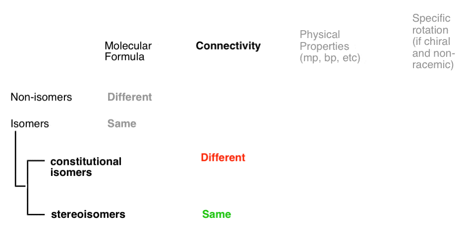
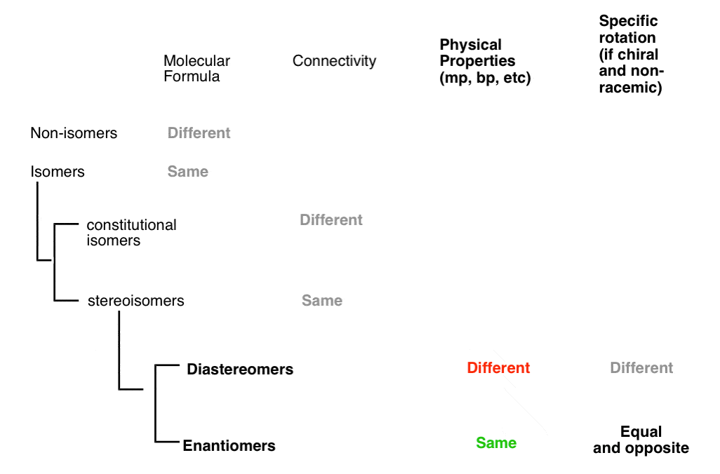
- A given pair of molecules can be isomers OR non-isomers
- A given pair of isomers can be constitutional isomers OR stereoisomers
- A given pair of stereoisomers can be enantiomers OR diastereomers
(on exams especially, there’s always the possibility that a “given pair of molecules” is actually the same molecule, drawn differently. We’ll cover that possibility too).
The flowchart maps out like this:
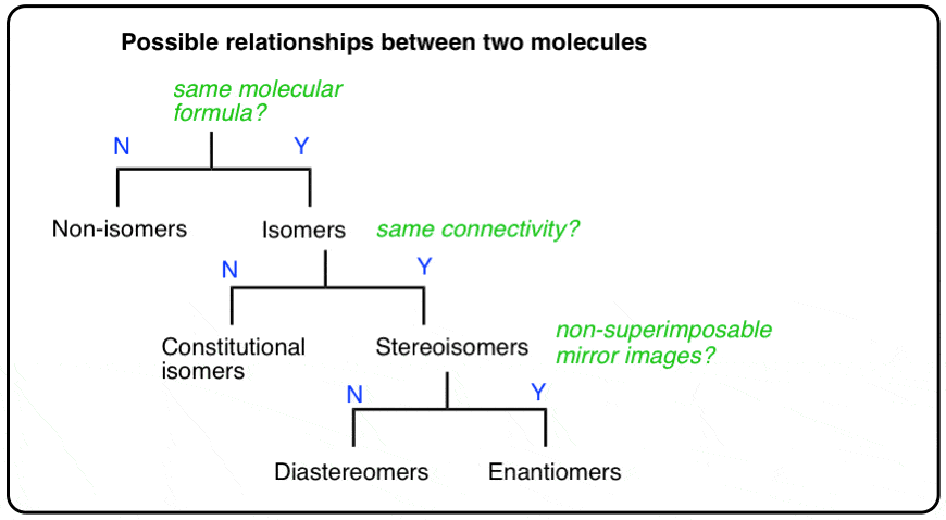
One key difference between families and molecules:
Through circumstances I will leave to the reader to figure out, it is possible for someone to simultaneously be both a father and a brother to the same individual.
Thankfully, we have no such problems in organic chemistry.
Two molecules might be stereoisomers of each other, but they can’t be stereoisomers and constitutional isomers of each other. The distinctions are clear.
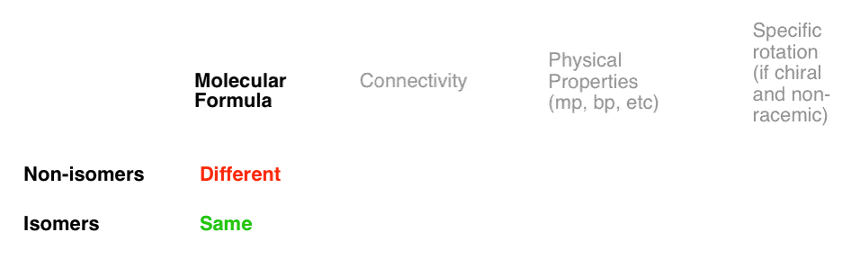
3. How To Distinguish A Pair Of Non-Isomers vs. A Pair Of Isomers
Isomers are two (or more) molecules that share the same molecular formula.
For some molecular formulae, no isomers exist. For example, there is only one possible isomer for CH4 (methane), C2H6 (ethane) and propane (C3H8), and only two are possible for C4H10 (2-methylpropane and n-butane).
As the number of carbon atoms increases, however, so does the number of possible isomers. For dodecane (C12H26), 355 isomers are possible. And it only goes up from there!
Despite sharing the same molecular formulae, isomers may have very different physical properties, such as boiling point, melting point, and chemical reactivity.
Take cyclohexane (b.p. 63 °C) and 1-hexene (80 °C) which both have the molecular formula C6H12. No matter how different their physical properties, or reactivities, their common molecular formula makes them isomers of each other.
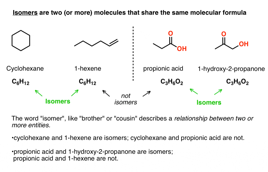
Likewise, propionic acid and 1-hydroxy-2-propanone share the same molecular formula, C3H6O2, making them isomers of each other (but not isomers of cyclohexane or 1-hexene, of course!).
This leads us to the next question. Let’s say that two given molecules are isomers. What kind of isomer are they?
Isomers divide neatly in to two categories: constitutional isomers (different connectivity) and stereoisomers (same connectivity, different arrangement in space). So what does that actually mean?
4. Types Of Isomers: Constitutional Isomers Have Different Connectivites
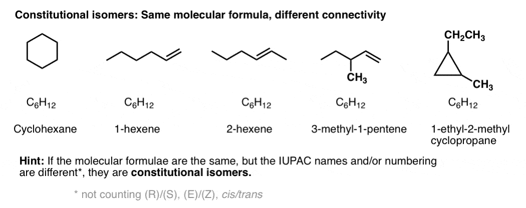
Constitutional isomers have the same molecular formula, but different connectivities.
The same parts, but arranged in different ways. To take this oldie-but-goodie example, switch a tail and a leg and you make isocats:

That’s fun, but is there a more rigorous way to think about connectivity?
Yes – from nomenclature. If two molecules with the same molecular formula have different connectivity, it will be obvious either in the locant (e.g. 1-hexene vs. 2-hexene), or in the substitutent(s), prefix, or suffix. e.g. 2-methylpropane vs. butane, or 1-pentanol vs. ethyl propyl ether.
I happen to find the following rule of thumb useful:
Constitutional isomers have the same empirical formulae but their core IUPAC names are different.
[By core IUPAC name I mean the locant(s), substituent(s), prefixes and suffix – everything except (R)/(S), E/Z, and cis/trans, basically.]
If the only point of difference in the names of two molecules is their (R)/(S) or (E)/(Z) designations (or cis/trans) then you’re dealing with stereoisomers (next section).
By way of an example, these 5 molecules are all constitutional isomers of each other. They have the same empirical formula (C6H12) but different connectivity. Note how the IUPAC names are all completely different as well.
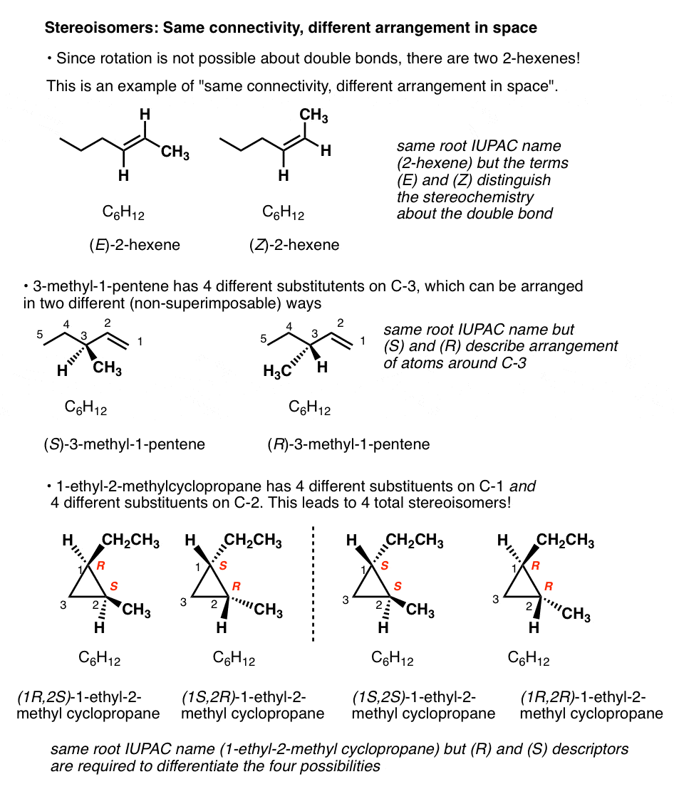
5. Types Of Isomers: Stereoisomers Have The Same Connectivity But A Different Arrangement Of Their Atoms In Space
There is only one way to connect C6H12 together to form cyclohexane, and only one way to connect the same atoms together to get 1-hexene.
But there are two ways to connect C6H12to give molecules with the names 2-hexene, and 3-methyl-1-pentene! And four ways to connect C6H12 to give 1-ethyl-2-methylcyclopropane!
(Quick way to identify a well-trained organic chemist: ask them to draw 2-hexene, and measure how quickly it takes them to say, “which one”?).
For example: there are two ways to arrange the hydrogens on the double bond of 2-hexene; when they are on the same side, we refer to it as cis (or Z); on the opposite side, trans (E). [See: Cis and Trans and E and Z] .
Since free rotation about the double bond is not possible, these are completely distinct molecules. They can be separated, put in different flasks, left on the shelf for years, and never interconvert. You can buy cis-2-hexene (95%) from Aldrich, leave it in the storage room for two decades, and never fear that it has turned into the trans form.
What kind of isomers are these? We can’t call them constitutional isomer, since they have the same connectivity (both are 2-hexene! ). We need another name. Since they differ in the arrangement of their groups in space about the double bond we call them stereoisomers.
Stereoisomers can also arise from tetrahedral carbon atoms that are attached to four different substituents (i.e. a “chiral” or “asymmetric” carbon) as in 3-methyl-1-pentene. There are 2 (and only 2!) different ways to arrange four different groups around a tetrahedral center, which gives rise to two molecules which share the same connectivity but differ in the arrangement of their atoms in space. These molecules may look the same, but they are actually non-superimposable mirror images (more on that a few paragraphs below).
6. Stereogenic “Elements” In Stereoisomers
A double bond capable of cis/trans isomerism as well as an “asymmetric” carbon atom are sometimes called “stereogenic elements” since they each give rise to a pair of stereoisomers (E or Z), or (R or S)
- A molecule that has 2 stereogenic elements can give rise to as many as (2 × 2) = 4 different stereoisomers. That is the case with 1-ethyl-2-methyl cyclopropane: (R,R), (S,S), (R,S), and (S,R).
- A molecule with 3 stereogenic elements can give rise to as many as (2 × 2 × 2) = 8 different stereoisomers.
- Generally, a molecule with n stereogenic elements can have up to 2n stereoisomers. (Probably the craziest known example in chemistry is palytoxin, which has 64 chiral centers, 8 double bonds, and about 1021 possible stereoisomers. )
One quick way to tell if two molecules are stereoisomers is if they have the same core IUPAC name but differ in their cis/trans, E/Z, or (R)/(S) designations.
7. Types Of Stereoisomers: Enantiomers vs. Non-Enantiomers (a.k.a. Diastereomers)
We’re not quite done. There’s a final important distinction to be made between two different types of stereoisomers.
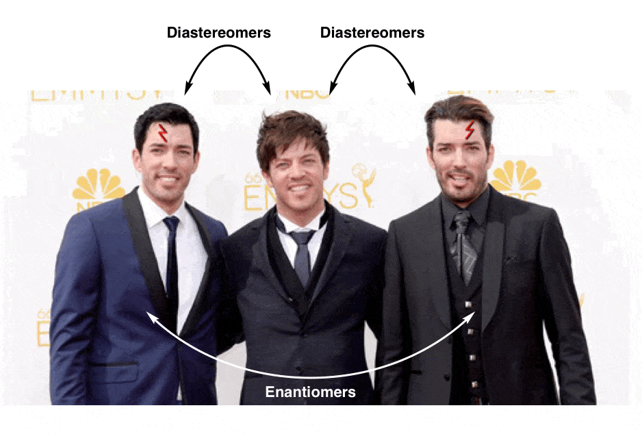
Why? Well, to push our family analogy just a little bit further… let’s talk about brothers:

(yes, there is a third Property Brother)
These three men are all brothers, but clearly there’s something special about the relationship between two of the three that merits its own category:
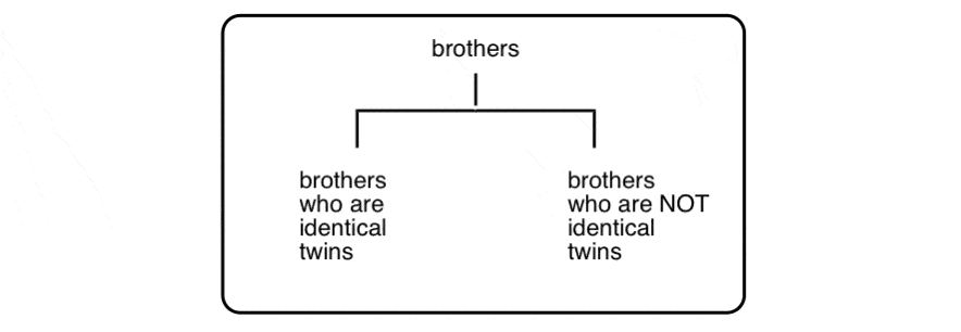
This is not unlike the distinction between diastereomers (stereoisomers that ARE NOT non-superimposable mirror images) and enantiomers (stereoisomers that ARE non-superimposable mirror images).
8. What Does “Non-Superimposable Mirror Image” Even Mean??
I will admit: the term “non-superimposable mirror images” seems to give people as much trouble as the “second cousin versus once-removed” thing. So let’s address this right now.
In our family analogy (above) we made “brothers who are identical twins” analogous to enantiomers, and “brothers who are not identical twins” analogous to diastereomers.
We need to tweak this analogy a bit.
In organic chemistry, two molecules that can be superimposed on each other, through rotation of bonds (i.e. conformational changes) or through rotation of the molecule itself, are considered to be the same molecule.
In other words, in organic chemistry, molecules that are “identical twins” are not isomers; they are considered to be identical copies of the same molecule.
A mole, after all, is 6.02 × 10²³ identical, superimposable molecules. And just like identical twins are still identical if one is sitting at a desk searching for available real estate that’s in your price range while the other is standing in a crappy kitchen gesturing with his hands trying to show you how it can be completely remodelled to fit your budget, molecules are still considered “identical” if they happen to be in different conformations, so long as they each pass through at least one conformation in which they are superimposable. [Advanced note: there is such a thing as conformers which are “locked” in such a way that they can’t interconvert, but it usually isn’t addressed in this course – see footnote]

Now, let’s make a little modification to our identical twins so that they go from being superimposable mirror images (= the same) to non-superimposable mirror images.
9. Property Brothers Season 13, Episode 13: “Lord Voldemort And The Property Of Chirality”
NARRATOR: Our client, “Lord Voldemort” said he was looking for a new evil lair with “good bones”, so we took him around town to look at some properties that fit his list of “must haves” and budget. Later that evening, after a few drinks, things got awkward.
LORD VOLDEMORT: Hey fellas, I actually have a new property YOU might be interested in
DREW AND JON: Jesus! What the hell is that thin-
LV: The property of CHIRALITY! Racemundum suorum!
ZAP! (flash of light)
DREW AND JON: Aaarrrggh!!
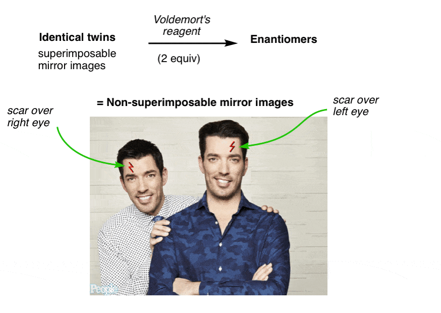
One has a scar over his left eye and the other has a scar over his right. No amount of twisting and turning on the floor in pain can possibly make them superimposable now.
They have become “enantiomers”: non-superimposable mirror images.
Since they are no longer superimposable, in chemistry terms they are no longer the same. Similar, yes! But not the same molecule.
What changed?
Voldemort’s Reagent
Before we added Voldemort’s reagent, each twin had a plane of symmetry along the middle of his body such that the left and right halves were identical. No more. Now the left half of each twin is different from the right half. We call this property “asymmetry”, or “chirality”.
The introduction of the scar “broke the symmetry” of each twin and introduced chirality.
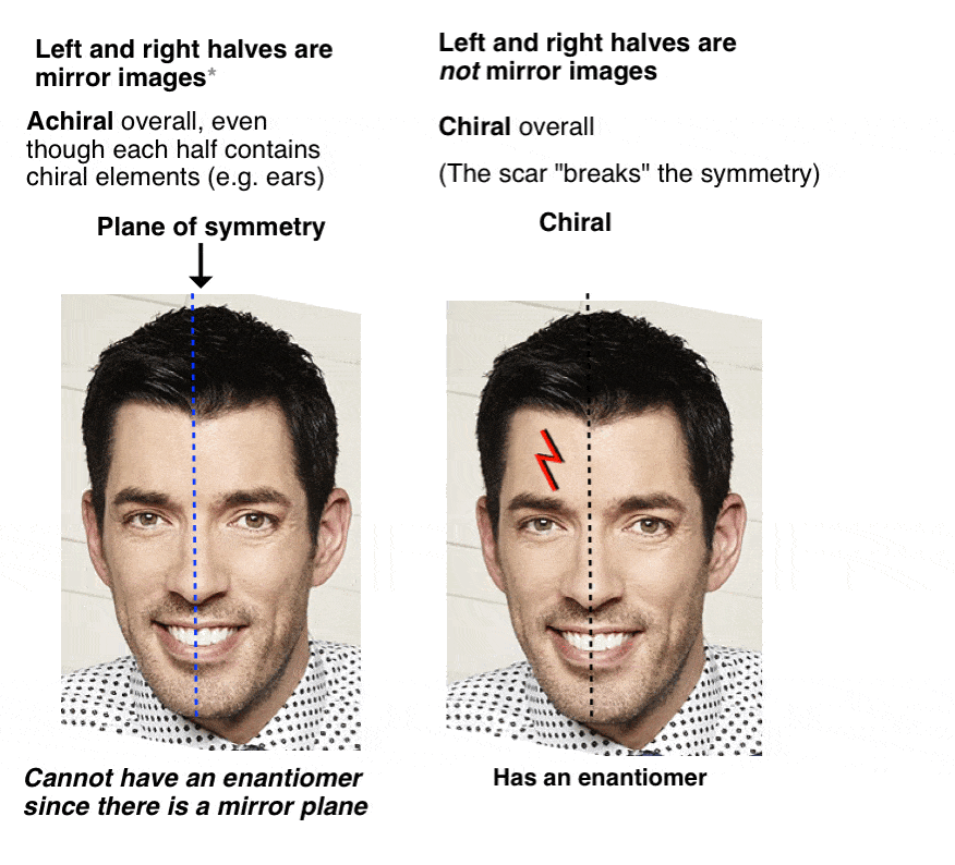
With molecules, the most common way to impart chirality is with a carbon bearing 4 different groups, as in 4-methyl-1-pentene, above. For this reason a carbon attached to 4 different groups is called a chiral center, or “asymmetric center”.

There are two (and only two!) ways to arrange 4 different substituents around a tetrahedral carbon. So a molecule with a single asymmetric center will exist as a pair of stereoisomers. To be more specific, it will exist as a pair of non-superimposable mirror images: enantiomers.
10. Enantiomers Have Identical Physical Properties Except for Optical Rotation
Earlier we described Louis Pasteur’s adventures with tartaric acid [See: Optical Rotation, Optical Activity, and Specific Rotation] where he discovered that a compound then known as “racemic acid” (from Latin racemus = “a bunch of grapes”) was in fact an equal mixture of two mirror-image forms of tartaric acid.
Separating these two isomers was hell on wheels, since they have identical solubilities, melting points, and other physical properties. Pasteur was only able to accomplish it through observing minute differences in the appearances of their salts, and picked them apart using tweezers and a magnifying glass.
The only physical property which differentiates these two isomers is that they rotate the plane of polarized light in equal and opposite directions.
With hindsight, we now know the structures of these two isomers of tartaric acid, and using the Cahn-Ingold-Prelog rules, have named them (R,R) and (S,S) tartaric acid.
These two isomers are mirror images of each other: Non-superimposable mirror images.
Just as with the placement of Voldemort’s scars, no amount of bond rotation can turn an (R) configuration into an (S) configuration, or vice versa. [See: Introduction to R and S – The Cahn-Ingold-Prelog Rules]
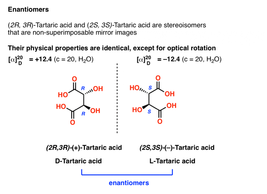
Note that they have the same core IUPAC name (2,3-dihydroxysuccinic acid, a.k.a. tartaric acid) but their R/S terms are completely opposite: (R,R) and (S,S).
This is an important clue in identifying enantiomers (and one we will discuss further in a future post):
Enantiomers will always have the same IUPAC names, and completely opposite (R/S) descriptors.
11. “The Third Property Brother”: meso-Tartaric Acid
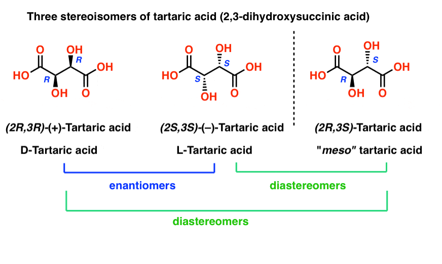
Tartaric acid has two asymmetric carbon centers, and we said earlier that a molecule with two asymmetric centers can have up to 22 = 4 stereoisomers. If (2S,3S) and (2R,3R) are two stereoisomers of tartaric acid, then what about (2R, 3S) and (2S, 3R) tartaric acid? These should also be stereoisomers, right?
When we draw out the structures of (2R,3S) and (2S,3R) tartaric acid, however, something quickly becomes apparent.
While they are indeed mirror images of each other, they are mirror images of each other in the same way that our (pre-Voldemort) identical twins are mirror images of each other:
They are superimposable mirror images, and therefore considered to be identical molecules.
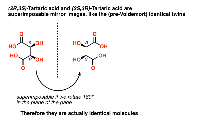
Therefore (2R, 3S)-tartaric acid and (2S, 3R)-tartaric acid are not enantiomers. They are actually two different ways of describing the same molecule, and tartaric acid only has three stereoisomers overall.
Wait. How can it be that a molecule can have chiral centers but not have an enantiomer?
12. Only Chiral Molecules Can Have Enantiomers
Just in the same way as our (pre-Voldemort) Property Brother had (chiral) left and right ears, but was achiral overall due to the internal mirror plane. Only chiral molecules can have enantiomers.
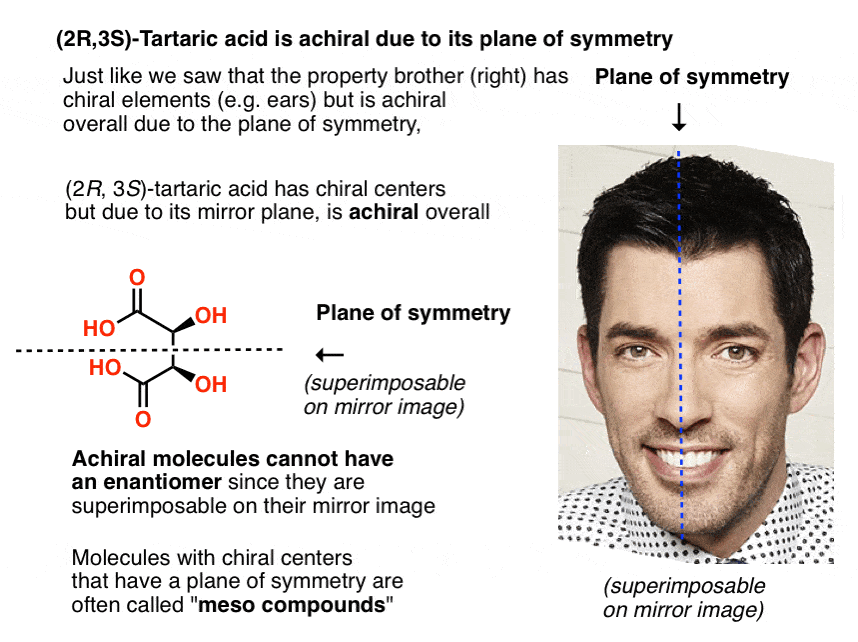
A molecule with an internal mirror plane – a plane of symmetry – is achiral and will not have an enantiomer.
Likewise, (2R, 3S)-tartaric acid has chiral centers, but possesses an internal mirror plane. The chiral center with the S configuration is the mirror image of the chiral center with the R configuration, and the other substituents are arranged symmetrically.
This stereoisomer of tartaric acid was known to Pasteur, since it could readily be separated from “racemic” tartaric acid owing to its different physical properties (solubility). Since its specific rotation (0°) was in “the middle” (meso = “middle” in Greek) between levo (–) and dextro (+) tartaric acid, it was given the name meso-tartaric acid.
Knowing what we do now, it makes sense that meso-tartaric acid has a specific rotation of 0°, since only chiral molecules rotate the plane of polarized light, and meso-tartaric acid is achiral.
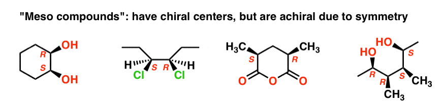
The name “meso” has been adopted more generally. A “meso compound” is a molecule that has chiral centers, but is achiral overall due the presence of an internal mirror plane.
This is why the qualifier “up to 22 stereoisomers” was used. A molecule with 2 stereocenters can have “up to ” 4 stereoisomers, but may have less than 4 if a meso form is present.
meso-tartaric acid is kind of like the third Property Brother: “the one who isn’t a twin”.
13. Diastereomers Are Stereoisomers That Are Not Enantiomers
So if (2R, 3R)-tartaric acid and (2S, 3S)-tartaric acid are enantiomers, how do we describe the relationship between each of these molecules and meso-tartaric acid?
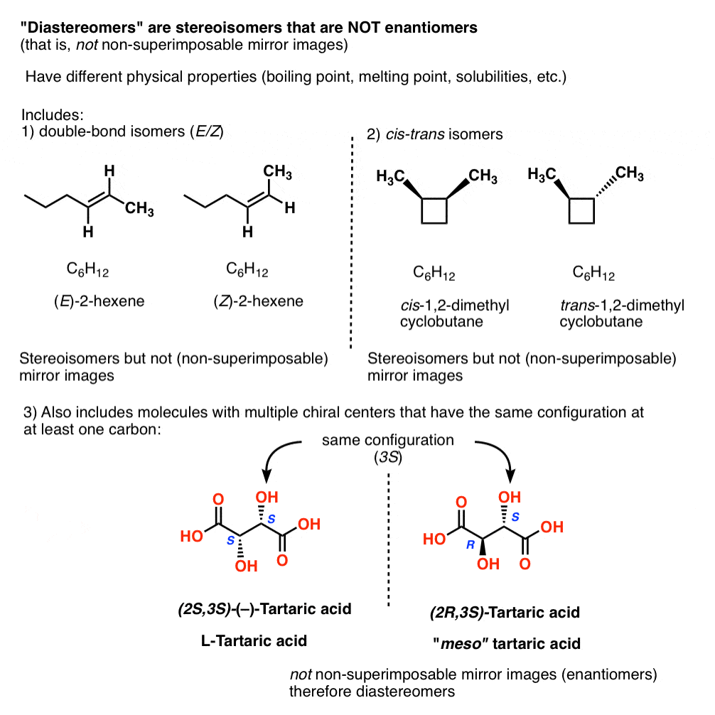
In organic chemistry, we call “stereoisomers that are not enantiomers”, diastereomers.
meso-tartaric acid is a diastereomer of both (2R,3R)-tartaric acid and (2S, 3S)-tartaric acid:
Other examples of “diastereomers” include:
- double bond isomers (E/Z)
- cis–trans isomers [see: cis and trans isomers of cycloalkanes]
- stereoisomers of molecules with multiple chiral centers that have the same configuration at (at least) one carbon
14. Diastereomers Have Different Physical Properties
Just as Pasteur found meso-tartaric acid relatively easy to separate from “racemic”-tartaric acid, diastereomers have different physical properties (e.g. boiling point, melting point, solubilities, etc.).
15. A Quick Way To Tell If Two Stereoisomers Are Diastereomers
A quick way to tell if two stereoisomers are diastereomers:
 if two stereoisomers differ in cis/trans or E/Z descriptors (e.g. cis-2-hexene and trans-2-hexene)
- if they have at least one identical R/S descriptor (as in (2S,3S)-Tartaric acid and (2R, 3S)-Tartaric acid (if all R/S descriptors are the same, they have to differ somehow in cis/trans or E/Z orientation to be diastereomers; otherwise they’re the same molecule!)
16. Watch Out For Trick Questions!
Last example, I promise.
Take the two molecules below. Are they isomers? If so, what kind of isomer are they?

The fastest way I know to answer this question is to try to name them both.
When we do this, we find that:
- the molecule on the left is E-(2R, 5R)-5-chloro-hex-3-en-2-ol
- the molecule on the right is E-(2R, 5R)-5-chloro-hex-3-en-2-ol
So how are they related?
- They’re not constitutional isomers (same connectivity!)
- But they’re not stereoisomers either (same E/Z and R/S descriptors !)
Therefore… they are the same! (Actually, they are different conformations of the same molecule, and we make the assumption that all conformations of the same molecule are interconvertible, unless told otherwise. ) see footnote.
17. Summary: Types Of Isomers
This has been a long, but hopefully comprehensive and illuminating post on the types of isomers.
In the next instalment we will learn a technique that – with practice – will allow you to quickly determine whether molecules are enantiomers, diastereomers, or the same.
Thanks again to Matt for co-authoring. Ask Matt about scheduling an online tutoring session here.
Notes
Generally we make the assumption that conformational isomers interconvert quickly on the timescale necessary to measure optical rotation.
For example, the two chair forms of cis-1,2-dimethylcyclohexane are actually enantiomers, but since they interconvert so quickly at room temperature, they are treated as if they are the same.
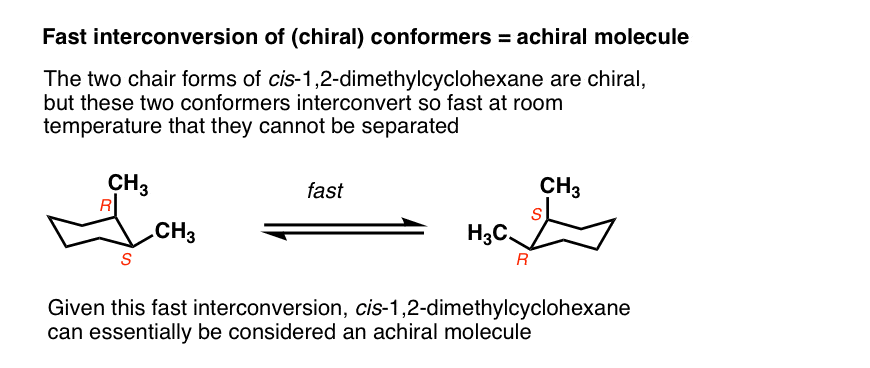
This is usually beyond the scope of introductory organic chemistry, but there are certain cases where this assumption isn’t valid.
A prominent example is 1,1-bi-2-naphthol (aka BINOL).
Conformer A (far left) can’t convert into conformer B (far right) without passing through a conformation where the two rings are coplanar (middle) , and the two hydrogens on each carbon (carbon 8) bump into each other. This presents a large enough barrier to rotation that each of these two conformations is “trapped” in its own state at room temperature and don’t interconvert.
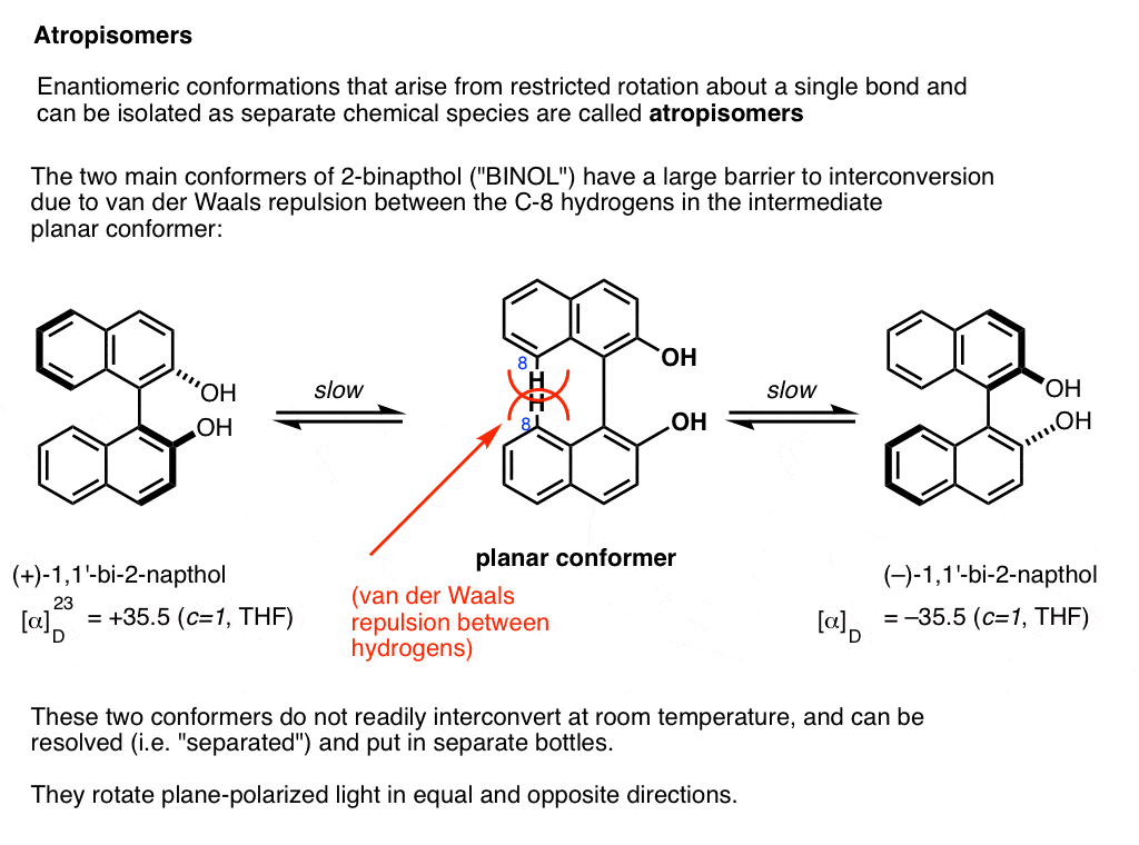
These two conformations are non-superimposable mirror images of each other in the same way that a left-handed and right-handed screw are non-superimposable mirror images of each other. They are said to have an “axis of chirality”.
The barrier between the two conformers is large enough that conformer A and conformer B can be resolved (separated) and put in different bottles.
This special case of isolable conformers is called “atropisomerism“.


 |
| images and electric field distributions of (a,d) Au nanosphere, (b,e) Au nanorod and (c, f) Au nanostar synthesized by wet-chemistry methods. |
“Terrella Cubica”: creating a Birkeland-like auroral simulator at Aalto University
Motivation
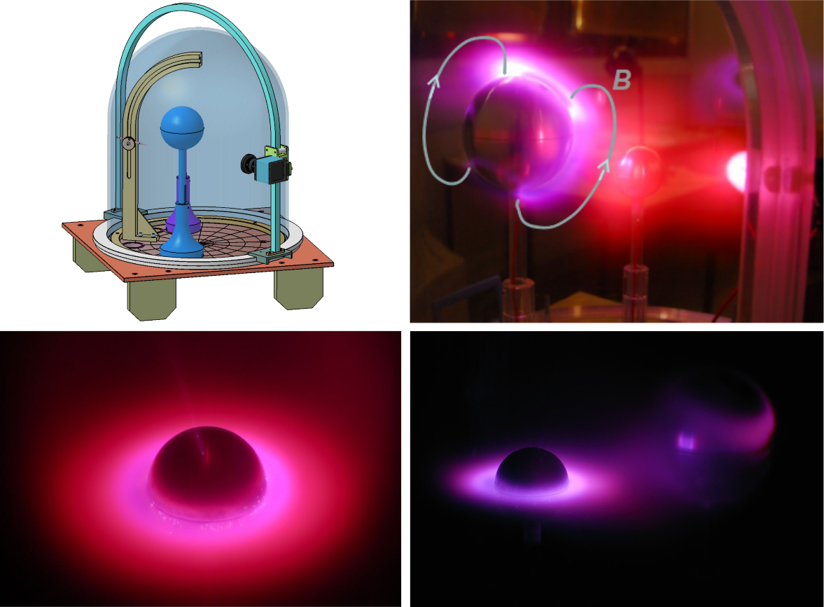
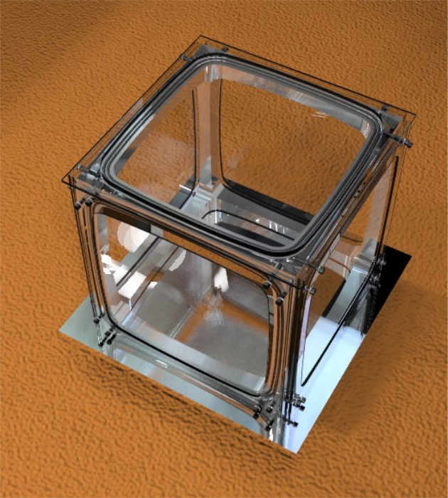
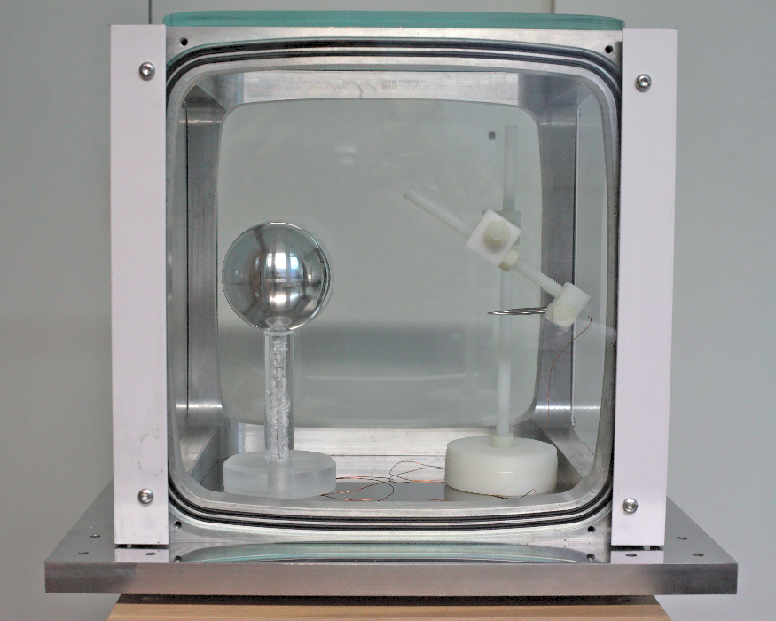
Based on Dr. J. Lilensten’s bell-jar design and as part of the Planeterrella European network, a revised design of a Planeterrella has been built in-house at Aalto University, consisting in a uniquely designed single-structure glass-aluminium vacuum chamber of cubic shape.
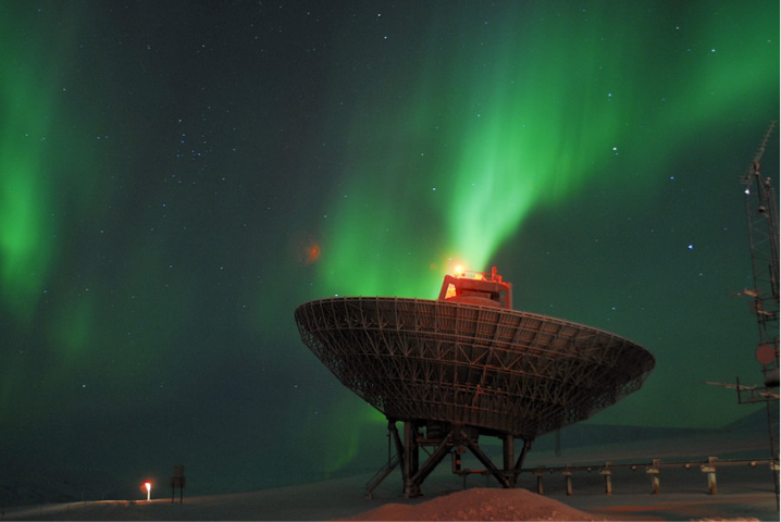
With code name Terrella Cubica, the aim is to support space physics teaching at the Aalto University's School of Electrical Engineering, by demonstrating plasma phenomena (auroral ovals, ring currents, etc.) usually only witnessed by instruments onboard space missions (Fig. 1).
The ingredients of the experiment: From Birkeland's Terrella...
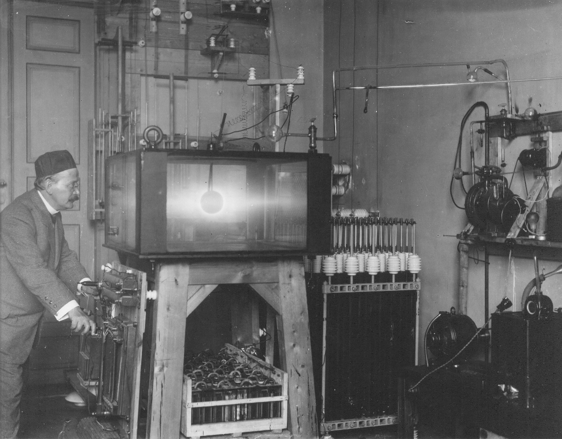
In 1902, the Norwegian physicist Kristian Birkeland started in Christiania (Oslo) a series of vacuum experiments to reproduce in the laboratory the auroral mechanisms he had theorised: he called them Terrella, "little Earth", in honour of W. Gilbert's magnetism experiments (Fig. 2).
The experiment is composed of:
- Vacuum chamber capable of reaching ionospheric-like pressures (~ 10-2 mbar)
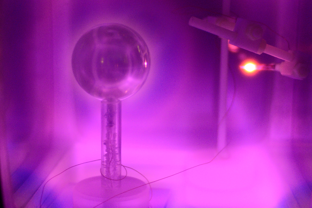
- Aluminium magnetised spheres, with dipolar magnets (1 T), to mimic Earth and other planets
- High-voltage power supply to mimic the electron flow (~ 1 kV, few mA)
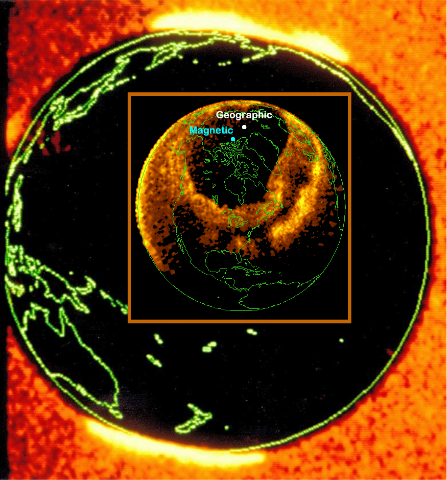
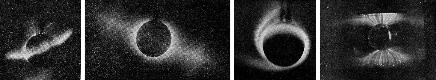
When these spheres are placed in a partial vacuum, an electric discharge is introduced between the anode and cathode, simulating electrons precipitating along magnetic field lines in the rarefied gas, hence creating auroral ovals in the Southern and Northern hemispheres (Fig. 3).
... to the Planeterrella as a teaching tool for space plasma physics
First created at Grenoble University (France), the modern Planeterrella experiment has since been remade 17 times in universities in Europe and the US.

It draws from Birkeland's heritage with many practical modifications that make it portable and accessible to Universities and public institutions. The main enhancement of the experiment is the use of several spheres to recreate Space Weather phenomena (Sun-planet or "exotic" star-exoplanet interactions). A typical experimental set-up is shown in Fig. 4 ("auroral ovals" mode).
All vacuum chambers are bell-shaped and standardised (Fig. 5).
The Planeterrella is organised as an international network bound by a Gentleman's agreement. Thanks to its success and several awards (EuroPlaNet, etc.), it has been seen and discussed by more than 50,000 people across the network.
Please visit us at:
planeterrella.osug.fr
Aalto's Terrella Cubica, one of the first Nordic Planeterrellae
Stemming from the original cubic-shaped plasma chamber of Birkeland, we have built at Aalto University a new prototype within the Planeterrella agreement, called Terrella Cubica (Fig. 6).
The experiment has been entirely created on site at the University as a single aluminium structure. The small pieces (spheres, pedestals) as well as the base plate were created from off-the-shelf raw materials by machining and by 3-D printers. Neodymium magnets of 1 Tesla intensity are used in the current setup.
Tests are under way at Aalto University. The experiment will be used to demonstrate basic phenomena encountered in planetary space plasmas such as the Lorentz force, the Debye length, the formation of ring currents or of upper atmosphere VIS-UV emissions.
References
- Brundtland, T., The Laboratory Work of Professor Birkeland in The Auroral Observatory, Thesis University of Tromsø, 1997.
- Egeland, A., and J. Burke, Birkeland, the First Space Scientist, Astrophysics and Space Science Library, Vol. 325, Springer, Dordrecht, 2005.
- Gronoff, G., and C. Simon Wedlund, 2011, Auroral formation and plasma interaction between magnetized objects simulated with the Planeterrella, IEEE Trans. Plasma Science, 39, 2712.
- Lilensten, J., M. Barthélemy, C. Simon, P. Jeanjacquot, and G. Gronoff, 2009, The Planeterrella, a pedagogic experiment in planetology and plasma physics, Acta Geophysica, 57, 220.
- Lilensten, J., et al., 2013, The Planeterrella experiment: from individual initiative to networking, Journal of Space Weather and Space Climate, 3, AA07.
- Rypdal, K. and T. Brundtland. The Birkeland Terrella Experiments and their Importance for the Modern Synergy of Laboratory & Space Plasma Physics. J. Physique IV, 1997, 07 (C4), 113-132.
Poster Presentation at the Finnish Physics Days 2015
The material on this page was first presented at the Finnish Physics Days 2015 as a poster. See the low-resolution copy here! Here are the authors:
T. J. Kärkkäinen1, C. Simon Wedlund1, E. Kallio1, M. Alho1 and J. Lilensten2
1Aalto University, Dept. of Radio Science and Engineering, School of Electrical Engineering, Espoo, Finland
2Institut de Planétologie et d’Astrophysique de Grenoble (UJF/CNRS IPAG), Grenoble, France
Modelling of Space Plasmas
In parallel to space remote and in-situ observatories, physical models have been developed to account for the observations and to predict the state of the space environment of the solar system objects. Several descriptions have been historically used, which are complementary: kinetic, fluid and hybrid. They are obtained by extending the kinetic theory of gases (see Boltzmann formalism) and the hydrodynamics of fluids to the plasma state of matter. The choice of the plasma description, either kinetic, hybrid or fluid, is intimately determined by the characteristic temporal and spatial scales encountered in the environment of study. This remark is illustrated in Illustration 3 when looking at the characteristic frequencies of the plasma, i.e., electron plasma frequency ωpe, ion plasma frequency ωpi, ion gyrofrequency ωci, Alfvén frequency ωa, and electron-ion collision frequency ωei.
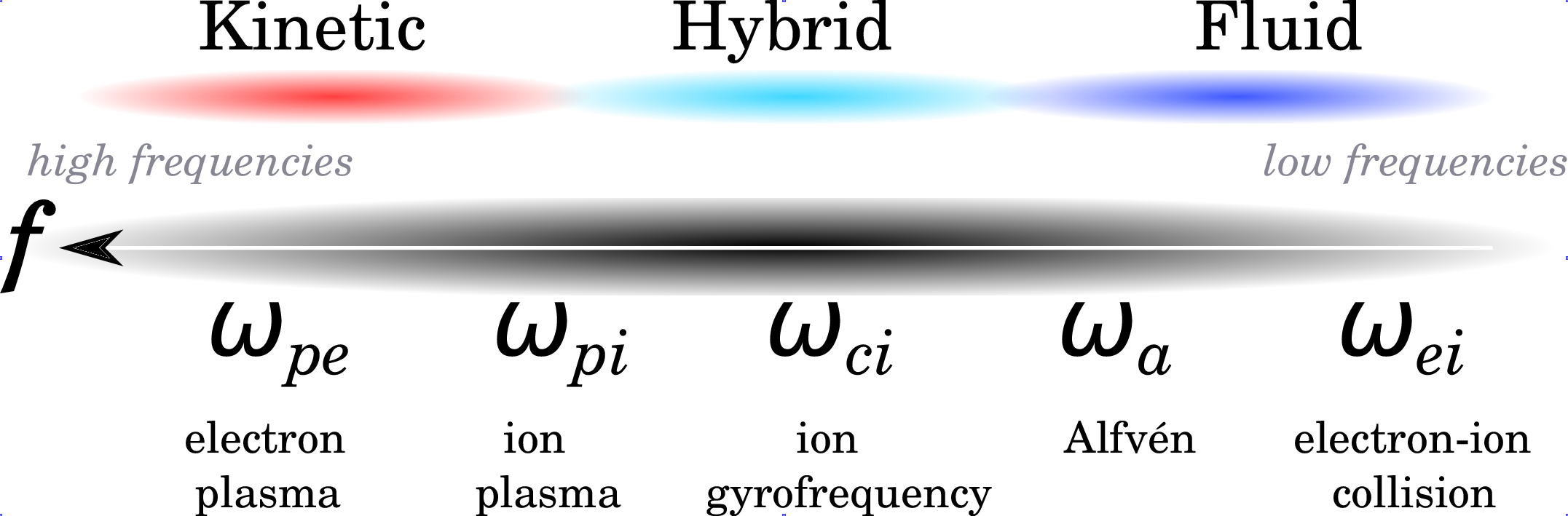
There are three basic self-consistent approaches to describe space plasmas: (a) kinetic, (b) hybrid and (c) fluid approaches:
- (a) Kinetic description:
The most fundamental description of plasma is the kinetic one where the position of particles is known in phase space, that is the space of all possible values of position and momentum variables. In the kinetic description, even the electron scale is accessible. Two different kinds of approaches may be used: [1] based on a distribution function and [2] based on individual (macro) ions. In case [1], the microscopic distribution function f in 6 dimensions (3 of space, 3 of velocity) represents all there is to know about the plasma state: in other words, f is the number of particles per unit volume having a given velocity at a certain time. The evolution of the plasma is most generally described by the Boltzmann dissipative equation, introduced by Ludwig Boltzmann in 1872. These kinetic models aim at precisely solving this equation. Macroscopic quantities such as number density, velocity, energy and heat transfer can be accessed by integrating the distribution function over velocity space. In the other approach [2] particles are modelled as “macro particles” or “particle clouds” which are accelerated by the Lorentz force, gravitational force, etc. Because kinetic simulations are computationally extremely demanding, most kinetic models are restrained to 1D studies. The HYB-em Particle-In-Cell (PIC) electromagnetic model developed at Aalto, based on the HYB-* platform but considering both electrons and ions as particles, is one such full kinetic model.
- (b) Hybrid kinetic/fluid description:
Hybrid models adopt the standpoint where ions are seen as particles and electrons become a massless fluid. The advantage of such a method is that the small-scale physics of ions is more accurately described since no assumption on the form of their distribution function is made. One of the main caveats of hybrid models is that they require a large number of particles to reach statistically significant results. Thanks to increasing computational resources, hybrid models have become more and more popular over the last 10 years. The HYB-* platform developed at Aalto belongs to this category and is described in more detail below.
- (c) Fluid description:
This description refers to any simplified plasma model that deals with quantities averaged over velocity space, hence, necessarily, with macroscopic quantities. Introduced by Hannes Alfvén as soon as 1942 in its ideal form, magnetohydrodynamics (MHD) assumes that the plasma behaves as a fluid embedded in its magnetic field upon which the Lorentz force acts. One shortcoming of this approach is that it implicitly assumes that the plasma is collisional with particle distributions having Maxwellian distributions, a condition which, in practice, is not met for smaller scale structures. The advantage of the MHD approach is that it is computationally much less expensive than kinetic and hybrid approaches and, therefore, it provides the possibility to obtain a good spatial resolution as well as to model large space regions.
Further reading:
- Recent review of available models and approaches:
- Kallio, E., J-Y Chaufray, R. Modolo, D. Snowden and R. Winglee, Modeling of Venus, Mars, and Titan, Space Science Reviews, DOI 10.1007/s11214-011-9814-8, 2011.
Distinction between Kinetic, Hybrid and Fluid plasma models, and introduction to kinetic simulations with differences in the modelled physics:- Winske, D., and N. Omidi (1996), A nonspecialist's guide to kinetic simulations of space plasmas, J. Geophys. Res., 101(A8), 17287–17303, doi:10.1029/96JA00982.
General textbooks about numerical simulations in plasma physics:C. K. Birdsall and A. B. Langdon, Plasma physics via computer simulation, Series in Plasma Physics, Taylor & Francis Ltd, New York, 2004, ISBN 9780750310253.
R. W. Hockney, J. W. Eastwood, Computer Simulation Using Particles, McGraw-Hill, New York, 1981, ISBN 9780852743928.
~~~&&&&&~~~
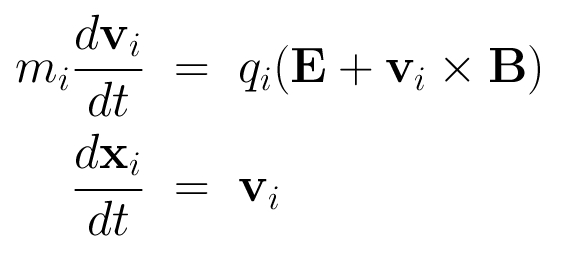
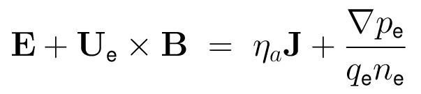
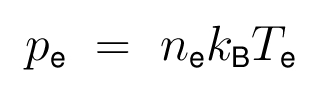
The Quasi-Neutral Hybrid model
The HYB simulation code is originally based on the quasi-neutral hybrid (QNH) description of plasma. Positively charged ions are treated explicitly as kinetic particles and electrons are modelled as a charge-neutralizing, massless MHD fluid. The ions and the electromagnetic fields are self-consistently coupled to each other. The implicit treatment of electrons by the fluid momentum equation defines the electric field. Physical laws that define the QNH model are the following:
- The dynamics of the ions in the electromagnetic field is governed by the Lorentz force:
- The electrons are considered implicitly as an inertia-less fluid by the fluid momentum equation:
- The ideal gas law as the electron equation of state is:
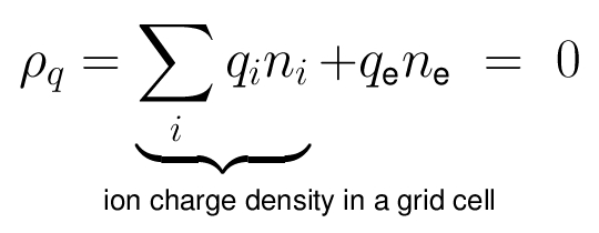
- The quasi-neutrality condition of the plasma is:
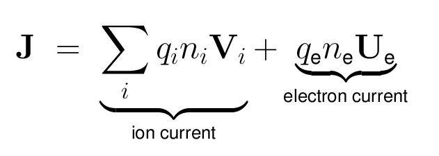
- The electric current density is defined as:
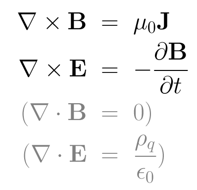
- Electrodynamics comes from the non-radiative Maxwell equations:
Summary
Assumptions:
- Quasi-neutrality
- Maxwell's equations solved consistently
- Ions accelerated by the Lorentz force and gravitation
- Magnetic field propagated using Faraday's law
Physical inputs:
- Object: Diameter and mass of the planet, gravity, intrinsic magnetic field, atmosphere & ionosphere, electric conductivity
- Flowing plasma (e.g., the solar wind): Density of ions, velocity distribution of ions, electron temperature, the ambient magnetic field (e.g., the Interplanetary magnetic field, IMF)
Solving the hybrid model
Example of the HYB-* platform: step-by-step
Equations of the QNH HYB model are solved by starting with initial values for the ions (positions and velocities) and the magnetic field in the simulation domain.
- The current density is obtained from the magnetic field by Ampère's law
- The electron charge density comes from the quasi-neutrality assumption in a grid cell
- The velocity field of the electron fluid is determined from the definition of the current density
- The electric field is calculated from the electron momentum equation
- Magnetic field is advanced by the Faraday's law
- Particles are moved and accelerated by the Lorentz force
Numerical solution: solving the hybrid model equations
Numerical approaches that are chosen which may differ from one model to another.
- HWA/HYB-* model
- The HWA/HYB-* platform is described in great technical detail in Kallio and Janhunen (2003):
Kallio E. and P. Janhunen, Modelling the Solar Wind Interaction With Mercury by a Quasineutral Hybrid Model, Ann. Geophys., 21(11), 2133-2145, doi:10.5194/angeo-21-2133-2003, 2003
Plasma Generators
Neutral beam injector for steady state superconducting tokamak
A.K. Chakraborty, ... S.K. Mattoo, in Fusion Technology 1996, 1997
2.1 Plasma generator
The plasma generator is a standard multipole bucket type source, which operates in the emission limited discharge regime. Filament temperature of each of the 24 filaments is independently controlled. The focused heat load due to backstreaming electrons increases upto 0.8 kW/cm2, while the remaining areas receive upto 0.4 kW/cm2. The stress/strain analyses, using ANSYS, shown in Fig. 2 predicts that a considerable increase in the fatigue life (∼105 cycles) can be achieved by using a flow rate of 80 g/s per channel at a pressure of 4 bar in the backplate. The arc chamber is water cooled for dissipating 0.2 kW/cm2 of heat at a flow rate of 240 g/s. Backplate is made of OFHC copper electroform jointed on SS plate. The operating surface temperature of the OFHC chamber is ∼150° C. The minimum filament lifetime is ∼2×10⁵ S, which allows approximately 40 days (4 shots a day) of operation.

Fig. 2. Strain distribution for 8MW/m2 concentrated & 2 MW/m2 distributed load.
Optimization of a large-area RF plasma generator
W. Kraus, ... E. Speth, in Fusion Technology 1996, 1997
A large-area plasma generator is being developed at IPP for the second injector of ASDEX Upgrade (AUG), scheduled for operation in 1997. The reliability of this source has been demonstrated last year in a demo series of 120 shots at the nominal beam parameters of 88 A, 55 kV, 5 s (1). Further attempts have been made to optimise transmission by improving the uniformity of the plasma density profiles in the extraction area. Variations of the magnetic configuration, geometrical conditions and operational parameters have been carried out. None of those did further improve the transmission so far. The parametric dependence of the transmission on beam energy, beam current/rf power and decel voltage is discussed including experiments up to 100 kV, using a modified extraction system.
Further attempts to reduce power losses and matching problems, caused by eddy currents in the Faraday shield, are under investigation at present.
~~~<^v>~~~
NEGATIVE ION EXTRACTION PHYSICS
M. Bacal, ... A.B. Sionov, in Fusion Technology 1996, 1997
2 EXPERIMENTAL SET-UP AND TECHNIQUE
The investigation has been performed in the hybrid multicusp plasma generator (Camembert III), which has been described in detail elsewhere1. The hybrid source contains three distinct regions : i) a driver region, located near the walls, containing the filaments; ii) an extraction region, which extends over all the central, field free region; iii) a weakly magnetized region with high Ni− / Ne, bounded by the plasma electrode, which contains the extraction opening (Ni− and Ne are the negative ion and electron densities, respectively). Here the joint action of the positive bias on PE and of the weak magnetic field (20 Gauss at most) results in the redistribution of the plasma components2,3. The photodetachment measurements effected at a distance from PE of up to 2 cm show a dramatic increase of the negative ion / electron density ratio, Ni−/Ne, from 0.5 to 10 (i.e. by a factor of twenty) when the PE bias, Vb, is enhanced from 0 to 2.5 V. In this case Ni− increases approximately by a factor of two, while Ne drops by a factor of ten (see Figs. 8 and 9 in Ref. 3). Note that the ratio Ni−/Ne does not exceed 0.1 in the center of the extraction region1.
The magnetic field in the neighbourhood of the plasma electrode is approximately parallel to this electrode; the electrons are magnetized on a distance of a few centimeters from it. A large fraction of the current into the extraction hole is transported by negative ions. The electrons, as lighter particles, flow to the periphery of the plasma electrode or to the periphery of the plasma chamber along the magnetic field lines.
The H” density, Ni−, was measured by the photodetachement technique, described in detail in Ref. 3 and 4. In this technique electrons are detached from the H− ions by means of a pulsed laser beam and detected by the cylindrical tungsten probe placed along the axis of the laser beam. The probe is biased positively relative to the plasma and therefore attracts the detached electrons. This results in a probe current pulse whose height is proportional to the H− density. The laser beam is provided by a Nd YAG laser (photon energy 1.2 eV).
The H− negative ion thermal energy was measured using the two-laser-pulse photodetachement technique4. This nonresonant optical tagging technique combines two succesive laser pulses with simultaneous Langmuir probe measurements. The first laser pulse destroys all the negative ions in its path by photodetachement. A second laser pulse fired shortly after the first along the same path destroys the negative ions which have originated from outside the laser path. The time evolution of Ni−(t) is established by making repeated measurements while varying the time delay between the two laser shots. The negative ion temperature T− is determined from the negative ion density recovery curve after the negative ions have been destroyed by photodetachement in a small cylindrical region.
~~~<^v>~~~
Fundamentals of Plasma Chemistry
Hiroshi Tanaka, Mitio Inokuti, in Advances In Atomic, Molecular, and Optical Physics, 2000
A ELECTRON COLLISIONS WITH MOLECULES
Electron collisions with molecules initiate the first step in plasma generation, as we saw in Section II.B, and therefore represent the most fundamental topic of plasma chemistry. Let us briefly discuss cross-section data for electron collisions as used in modeling studies (Tanaka and Boesten, 1995; Christophorou et al., 1996; Christophorou et al., 1997; Christophorou and Olthoff, 1998; Morgan, 1999). One uses the notion of the cross section to express the probability of a collision of an electron with a specific molecule. Suppose that a beam of unit flux of electrons of a fixed momentum enters a gas consisting of a single chemical species at unit density. Then, the number of electrons scattered into a solid-angle element around the direction given by angle θ measured from the direction of incidence is called the differential cross section σ(θ). This differential cross section can be further classified in terms of the quantum state n of the molecule left after the collision; thus, the number of electrons scattered in the same way as above and leaving the molecule in state n is called the differential cross section for the excitation to state n and is designated by σn(θ). When the state of the molecule after the collision is the same as that before the collision, we call the collision elastic, and the differential cross section for this process may be written as σ0(θ). The integral of the differential cross section over all possible scattering angles is the (integrated) cross section qn, which is a function of the electron kinetic energy, i.e.,

qn=2π∫σnθsinθdθ,
where the factor 2π comes from integration over the azimuthal angle. The integral of the differential cross section σ0(θ) multiplied by 1 – cos θ is the momentum-transfer cross section

qm=2π∫σ0θ1−cosθsinθdθ,
which is a function of the electron kinetic energy and determines the mean energy transferred to the translational motion of the molecule upon elastic scattering of an electron. The integral of the cross section qn multiplied by the electron speed v and the distribution f(x,v, t) is the reaction rate for electron collisions.
Figure 5 (Kurachi and Nakamura, 1990) presents a survey of electron collision cross sections of CF4. In addition to the momentum-transfer cross section qm, it shows the vibrational-excitation cross sections qv3 and qv4 (for two different vibrational modes), the (total) electronic-excitation cross section qe, the dissociation cross section qdn, the electron-attachment cross section qa, and the (total) ionization cross section qi. Each of the cross sections is a function of the electron kinetic energy and reflects the physics of the collision process, which is being clarified by theory. The cross sections designated as “total” can be discussed in greater detail in terms of different contributions, which are designated as “partial” cross sections.

Fig. 5. Cross sections (in units of cm2) of CF4 for electron collisions as functions of electron energy (in eV), according to Kurachi and Nakamura (1990).
For chemical etching, polyatomic halogen-bearing molecules are often used. Electron collisions with these molecules often lead to negative ions through electron dissociative attachment,

e+CF4→CF4−*→CF3−+F or CF3+F−,
which usually occurs via a temporary negative-ion state in competition with vibrational excitation. (See the region near 8 eV in Fig. 5.) The negative ions thus produced tend to be accumulated in the plasma, and play the role of scavenger of excess electrons in the plasma. They also contribute to reducing the electric charging of the base surface. Attachment of electrons of thermal energy also occurs often with halogen-containing molecules; measurements with electrons in the microelectron volt domain (Dunning, 1995) are beginning to be made.
The determination of electron-collision cross sections over a broad range of kinetic energy cannot be accomplished in a single experiment, and requires the use of many different methods that are complementary to one another (Morgan, 1999). The methods include the electron-beam method (Trajmar and McConkey, 1994), the electron swarm method (Crompton, 1994), the beam attenuation method, and the microwave-cavity method used with pulse radiolysis (Shimamori, 1995). The electron-beam method permits measurements of the cross section for each channel of excitation distinguishable within the energy resolution, its angular dependence, and its dependence on the electron kinetic energy. However, in general, arriving at absolute values of cross sections is not straightforward. The swarm method determines macroscopic parameters describing the transport of electrons in a gas, and one deduces a set of cross sections consistent with the measured parameters from an analysis of electron transport through the solution of the Boltzmann equation or Monte Carlo simulations, as discussed in Section III.B. Certainly the analysis provides an opportunity for a comprehensive survey of cross-section data (Christophorou et al., 1996; Christophorou et al., 1997; Christophorou and Olthoff, 1998). However, great care is required to make certain that all the major processes are properly accounted for. The beam attenuation method determines the grand total cross section, that is, the sum of the elastic-scattering cross section and all inelastic-scattering cross sections, absolutely and often reliably. The grand total cross section is useful as a test of a cross-section set and as an upper bound for an individual cross section. The microwave-cavity method allows one to derive electron-attachment and other cross sections at thermal energies (Shimamori, 1995).
~~~<^v>~~~
MATERIAL COATING USING ELECTROMAGNETICALLY ACCELERATED PLASMA JET
Hirokazu Tahara, in Novel Materials Processing by Advanced Electromagnetic Energy Sources, 2005
Abstract
In magneto-plasma-dynamic (MPD) arcjet generators, plasma is accelerated by electromagnetic body forces. Two types of MPD arcjet generator were developed for applications to mullite, zirconia, titanium-nitride and silicon-nitride sprayings. The MPD spray process could successfully form dense, uniform and hard ceramic coatings. In titanium nitride reactive spraying, plasma diagnostic measurement and flowfield calculation were also carried out. A large amount of N and N+ was expected to be exhausted with a high velocity from the MPD generator. Both the electron temperature and the electron number density were kept high at a substrate position compared with those for conventional low-pressure thermal sprayings. A chemically active plasma with excited particles of N+, Ti, Ti+ and Ti2+ was considered to contribute to better titanium nitride coatings. The coating characteristics showed that the MPD arcjet generator had high potentials for material spraying.
~~~<^v>~~~
Atomic, Molecular, and Optical Physics: Electromagnetic Radiation
James F. Young, in Experimental Methods in the Physical Sciences, 1997
1.4.3 Short-Pulse-Length Pumping
There are several advantages to using short-pulsed lasers for plasma generation. Damage and energy storage limitations force laser apertures and system cost to increase with pulse energy, usually much faster than linearly. Short-pulse excitation, therefore, offers a means of achieving the required high focal intensities for plasma heating with a modest laser investment. In addition, the temperature and radiation of laser-producedplasmas generally track the time behavior of the pump pulse. The rise times are driven by the very high laser heating rates and follow the pump pulse, but the plasma decay time is determined by cooling rates that are independent of the laser pulse and typically limit the minimum radiation pulse length to ~10 psec. Nevertheless, short-pulse excited plasmas offer a unique source for time-resolved studies at very short wavelengths. But the laser-plasma interaction is not independent of time scale. As noted earlier, the plasma scale length decreases directly with pulse length, and that, in turn, decreases the fraction of laser energy absorbed. Figure 10 illustrates this reduction in conversion efficiency for pump pulse lengths below about 200 psec. Physically, it takes time for a plasma to form and expand, and that time is independent of the exciting pulse duration. During a very short laser pulse, there is insufficient time to form a significant volume of low-density plasma where light can be absorbed. Instead, most of the light is reflected from a near-solid density plasma at the target surface.

Fig. 10. Conversion efficiency into the 120–285 eV spectral band as a function of pulse length. The prepulse arrives at the target about 1.5 nsec in advance of the main pulse.
From reference [63].
One approach to reducing this problem is to apply a prepulse to the target that initiates a small plasma [31, 61–63]. This plasma then expands during the interval until the main pulse arrives, resulting in a large plasma volume with a long scale length that can absorb light efficiently. Figure 11 shows the significant improvement that can result by using just a small fraction of the pump energy, about 10%, for the prepulse. In these experiments the exact interval between the prepulse and the main pulse was not critical. Delays in the range of 1 to 2 nsec, corresponding to a plasma expansion of ~10 pm, were optimum. Experiments with very-high-in-tensity, 1017 W cm−2, subpicosecondpulses yielded short optimum delays of about 20 psec [29]. In this parameter range, the coupling of plasma expansion, heating, and cooling processes are quite different.

Fig. 11. Enhancement in plasma x-ray yield versus the fractionof main pulse energy used for the prepulse.
From reference [63]. .
Another approach to increasing efficiency when using ultrashort pulses is to use a target surface that has a built-in density gradient to reduce pump reflection. Etched microgrooves and colloidal porous coatings have been used successfully [64]. This technique increases the absorption of the pump laser energy into a plasma that is near solid density and results in high conversion efficiencies to x-rays above 1 keV energy.
~~~<^v>~~~
Development of a Novel Compact RF–Source
B. Heinemann, ... W. Szcepaniak, in Fusion Technology 1996, 1997
1 INTRODUCTION
For many years now different types of large area, rf-driven plasma generators have been developed at IPP. They could replace the so far used arc discharge sources, whose tungsten filaments have to be renewed periodically. With this respect the rf-source would be a significant advantage for ITER.
So far the best results were delivered in a configuration, in which the rf-antenna is separated from the plasma by a quartz vessel. A Faraday shield inside the quartz vessel is used to prevent erosion of the quartz and deposition of SiO2 onto the extraction grids. Furthermore a vacuum vessel outside the quartz vessel is needed as the quartz can not withstand the atmospheric pressure.
This design was successfully tested in the full “PINI”-size (32×61 cm2, 19 cm long, 331 volume) at the testbed. A series of 120 pulses was carried out, operating with nominal parameters of 55 kV, 88 A, 5s (H+). The needed rf-power was about 110 kW (Ref. 1).
Based on these results it was decided to equip the second injector on ASDEX Upgrade with these sources. It will go in operation in autumn 1997.
For future applications (e.g. negative ions, ITER) a new type of rf-source is under development, which simplifies the mechanical construction, erases some of the existing problems and rises the experimental flexibility: it combines all the functions of the different walls (vacuum tank, quartz vessel and Faraday shield) within one single wall. This means the source vessel is now a self supporting vacuum tank with an integrated Faraday screen, permeable to rf-waves but leak tight. The rf-coil as well as the permanent magnets are now outside under air and easily accessible. The paper first describes the design of the advanced rf-source compared to the present design. Then a description of the status of development, tests and results will be given. Finally the next steps, which are planned, will be outlined.
~~~<^v>~~~
Atomic, Molecular, and Optical Physics: Charged Particles
G.D. Alton, in Methods in Experimental Physics, 1995
3.4 Electron–Cyclotron Resonance and Microwave Ion Sources
During the past several years, multiply charged ion sources based on the ECR principle have been developed. The ECR source technology has advanced steadily over the years, driven by needs for high-charge-state beams for high-energy applications. The ECR ion source was first used by Geller et al. for multiply charged ion beam generation [107, 108], and the technology has continually grown. ECR ion source technology for multiply charged ion generation has rapidly advanced due to developments at several laboratories [109-111]. Reviews for high-charge-state ECR ion sources are given in Lyneis and Antaya [112] and in another chapter in this volume [113], The principles of operation and history of ECR source developments for multiply charged ion beam generation are discussed in Jongen and Lyneis [114]; scaling laws for high-charge-state ion wave generation have been postulated by Geller [115]. A new ECR concept for multiply charged ion beam generation has also been proposed [116]. Taylor [117] reviews high-current, low-charge-state ECR ion sources. Computational studies have been utilized to design an ECR ion source based on a new magnetic-field geometry for multiply charged ion beam generation. The properties of ECR plasmas generated by low-frequency microwave power have been measured by a number of investigators, including Amemiya et al. [118] and Popov [119]. A major advantage of this source concept is that the bombarding and ionizing electron current is generated from the plasma itself, and there are no emissive electrodes which can erode as a result of ion bombardment and thus limit the lifetime of continuous operation.
3.4.1 Principles of an ECR and Microwave Ion Source
An ECR and microwave ion source comprises a multimode cavity that serves as the plasma generation and containment cavity. Magnetic mirror coils are situated at the inlet and ion-extraction ends of the cavity to confine the plasma in the axial direction. Multicusp, magnetic fields are usually used to assist in containing the plasma in the radial direction. A high-frequency cavity is positioned on the inlet side of the source, and high-frequency power of several gigahertz is used to produce a plasma from the gaseous-feed material that is metered into the source. The operating pressure in this so-called first stage of the source is ~10−3 Torr. After generation, the plasma drifts down the axial magnetic field gradient into a second cavity of the source, where the electrons are resonantly excited by the high-frequency field at a frequency
(3.97)ωRF≅ωc=eBme,
where ωRF is the excitation frequency, ωc is the electron cyclotron frequency, e is the magnitude of the electronic charge, B is the magnetic flux density, and me is the mass of the electron. Wherever the resonance condition of Equation (3.97) is satisfied, the electrons are stochastically heated, a small fraction can actually attain energies of a few to several kilo-electron volts, and they are thus capable of removing tightly bound electrons from heavy ions. The pressure in this so-called second stage of the ECR source is ~10−6 Torr.
Ionization occurs principally by single-electron removal with contributions from multiple-electron removal and inner shell vacancy creation, which may result in Auger electron ejection. Single-electron-loss processes are believed to dominate so that multiple collisions are necessary to produce highly charged ions. Thus, it is necessary to make the product neτi as large as possible, where ne is the electron density and τi is the containment time of the ion beam. Power can be coupled into the plasma until the plasma density reaches the critical value nc, at which time the electron plasma ωρe, excitation ωRF, and electron cyclotron ωc frequencies are equal, i.e., ωRF = ωc = ωpe. The plasma frequency is related to the critical plasma density through the following expression,
(3.98)ωpe=(nce2ε0me)1/2;
therefore, nc∝ωRF2 However, for a fixed magnetic field design configuration, ωRF and thus nc are limited by the attainable magnetic field B in the multimode cavity of the source.
To increase the number of highly charged ions, multiple-stage sources (usually two stages) have been developed so that the ion containment time τi can be increased to values compatible with those required for production of higher-charge-state ions. Ion-ion collision recombination processes tend to lower the charge-state distribution at higher operating pressures, and, therefore, differential pumping is used so that lower pressures can be maintained from stage to stage. Ions diffuse along the axial field gradient and flow from stage to stage until they are extracted. The RF power generator usually has the capability of producing a few hundred watts to a few kilowatts of power. The power may be pulsed with typical widths of tens to hundreds of milliseconds at variable repetition rates or be continuous.
Electrons at the resonance frequency are excited essentially in a direction perpendicular to the axial magnetic field so that their energy perpendicular to the field is much greater than that parallel to the field, or T┴ ⪢ T||. Because of the direction of excitation and the magnetic-mirror geometry, the electrons are very effectively trapped, and, therefore, it is possible to bombard ions continually with several amperes of electron current during their diffusion along the field. Ions arriving at the outlet end of the source diffuse through an aperture into a field region where they are extracted. Total current densities of a few amperes per square centimeter have been extracted from the single-stage source. While the source is perhaps the most efficient and best method for producing CW beams of highly charged ions for injection into high-energy acceleration devices, e.g., the RFQ linear accelerator and cyclotron, low-charge-state, single-stage ECR sources have also been developed for use in producing beams of rare isotopic elements [120,121].
According to Equation (3.98) the maximum plasma density or critical density that can be achieved under ECR conditions is limited by the plasma frequency ωpe. In order to avoid cutoff at ωpe, the power source frequency ωRF should be chosen such that ωRF > ωc. However, the density limitation can be overcome by operation in the so-called “overdense” mode [122, 123], This means that a low-cost 2.45-GHz power source can be used to achieve densities far exceeding the theoretical ECR limit of ne = 7.45 × 10¹⁰/cm3. For example, densities of ne ≥ 3 × 10¹³/cm3 have been achieved using a 2.45-GHz magnetron power source [124]. The magnetic field necessary to excite an “overdense” plasma, however, must be increased over that required to meet the ECR condition.
3.4.2 Low-Charge-State ECR and Microwave Ion Sources
Several low-charge-state microwave ion sources which operate in the overdense mode have been developed. Multiple-aperture sources have been developed for fusion-reactor-related research, modification of material surfaces, and SIMOX applications [125], as well as slit-type sources such as those described in Sakudo et al. [126], which are suitable use in ionmplantation or electromagnetic isotope separator
applications. A schematic representation of the slit-type source of Sakudo et al. [126], developed for ion implantation applications, is shown in Figure 32. In this source, the discharge is initiated and sustained by microwave-induced excitation and ionization of the gaseous feed material. The frequency of the microwave generator is 2.45 GHz. Waveguide techniques are used to optimally transmit and couple several hundred watts of microwave power to the discharge volume, which is effective in producing a highly ionized plasma. A dielectric plate is utilized as a seal against atmospheric pressure. Analyzed 10-mA beams of P+ from an exit aperture of 2 × 40 mm2 have been observed. Because of the nature of the plasma-generation technique, the source has a very long lifetime. The principal problem which limits lifetime is backstreaming electrons which strike the dielectric plate located in the rear of the source and ultimately cause vacuum leaks. A comparison of the performance of this source with those of selected Freeman, Calutron, Calutron-Bernas, and microwave sources is made in Table III.

Fig. 32. Schematic drawing of the high-intensity, slit-aperture, microwave source described in Sakudo et al. [126].
Table III. Comparison of the Performances of Calutron, Calutron/Bernas, and Sakudo Ion Implantation Sources
Calutrona Calutron/Bernasb Freemanb Sakudoc
Ion species B + P+ B+ P+ B+ P+
Source gas BCl3 P0 BF3 P0 BF3 P0
Extraction area (cm2) 3.2 3.2 1.2 1.2 0.8 0.8
Arc voltage (V) 100 80 100 89 100 NA
Arc current (A) 4.5 3.0 5.5 3.0 4.5 NA
Microwave power (W) NA NA NA NA NA 300
Extraction voltage (kV) 35 35 20 20 35 30
Current density (mA/cm2) 65-100 65-100 44 35 44 50
Gas flow (atm cm3/min) 10-12 1-2 7 1 ~7 0.1-0.5
Lifetime (hr) 60-80 60-100 40-50 43 40-50 ≥100
a
Oak Ridge National Laboratory, TN
b
Eaton Corporation, Beverly, MA [84].
c
Sakudo microwave.
Oxygen is particularly deleterious to hot-cathode sources, the use of which may reduce the lifetime to a very few hours due to the chemical reactions between the oxygen feed gas and the hot Ta or W filaments traditionally used in such sources. The microwave or ECR ion source has an advantage over most conventional sources in that it lacks a filament, the component which limits the ultimate functional lifetime of the source. Thus, stability of operation with reactive gases can be easily achieved due to the microwave or ECR ion source’s nonfilament structure while simultaneously they have the benefit of long lifetime. A few sources have been successfully developed for corrosive feed materials processing such as oxygen [127-129]. O+ beams are important in the semiconducting materials industry for use in SIMOX technology. These sources have the capability of producing O+ currents exceeding 100 mA as required for use in commercial ion-implantation devices. Figure 33 displays a source developed for this application which generates O+ beams exceeding 138 mA at current densities exceeding 150 mA/cm2.

Fig. 33. Schematic diagram of the high-intensity, O+, microwave source described in Torii et al. [127].
A multicusp-field source which uses microwave plasma cathodes to supply electrons for ignition of the primary plasma in the cusp-field region of the source has been developed [130]. The plasma in the cathode region of the source is ignited by three rod coaxial-type antennae located on the back plate of the source which are driven at 2.45 GHz under ECR conditions. Total beams of Ar (exceeding 230 mA) and O (exceeding 130 mA) have been extracted from the source with a multiple-aperture emission diameter of 115 mm. The lifetime of the source, which is determined essentially by the lifetime of the antenna used to produce the microwave plasma, exceeds 100 hr.
A low-emittance, high-intensity ECR (microwave) source operating with a 2.45-GHz magnetron has been developed for producing high-proton-ratio H+ beams for postacceleration with an RFQ injector [131]. Proton fractions up to 90% and total extracted beam densities up to 350 mA/cm2 have been extracted from a 4-mm-diameter single-aperture source. The rms emittance of the source for a total beam intensity of25 mA is reported to be 1.55 π mm · mrad (MeV)1/2.
The compact microwave source, illustrated schematically in Figure 34, uses a quartz tube [132]; the plasma is produced with a 2.45-GHz magnetron power supply which couples power through the quartz tube. Both solid materials and gases have been generated with the source. The source produces hydrogen ion densities of 200 mA/cm2 with an 80% proton fraction.

Fig. 34. Schematic diagram of a microwave ion source similar to the source described in Walther et al. [132].
~~~<^v>~~~
Evaluation of an Advanced Silicon Doped CFC for Plasma Facing Material
C.H. Wu, ... G. Vieider, in Fusion Technology 1996, 1997
(f) Chemical erosion and stability of Si dopant
The measurements of chemical erosion were carried out in two different facilities: a, Plasma Generator Device PSI-1 (flux density 1018 cm−2 s−1), b, High Current Ion Beam Source (flux density 3 × 10¹⁵ D+ cm−2 s−1).
At plasma Generator Device PSI-1, the chemical sputtering yield was measured dynamically (during temperature rise) with a calibrated mass spectrometer and the CH-band intensity as well as by the weight loss method. The results of mass spectrometry agree well with the values obtained by weight loss method. It is seen, that the maximum chemical sputtering of Si-doped CFC(NS31) is at least factor 2 lower than that of undoped CFC(DUNLOP 3D).
At High Current Beam Source, the chemical sputtering yield was determined by weight loss method. It is clear that the yield of Si-doped CFC is about factor of 2 lower than that of undoped carbon.
To investigate the stability of Si dopant surface compositon specimens were analysed pre and post-heat treatment. Before the heat treatment, the Si concentration at surface is quite inhomogeneous. After the sample has been heated up to 1800 K for 2 hours, a loss 1-5% of Si has been investigated and enhancement of Si concentration has been observed after heat treatment. The chemical sputtering yield of heat treated sample at 800 K is about a factor of 5 smaller, and the sputtering yield at 40 eV and 300 K is 3-5 times smaller than that of undoped carbon.
~~~<^v>~~~
Vacuum Arc Initiation and Applications
B Jüttner, in High Voltage Vacuum Insulation, 1995
15.2.3(iv) Cathode Spot Theories
A theoretical treatment of arc cathode spots must deal with a number of variables describing electron emission and plasma generation:
(i)
Electron emission density, depending on surface temperature and electric field.
(ii)
Surface temperature, determined by the heat balance at the cathode. The latter depends on the geometry of the heated surface region, on heating by impinging plasma ions and plasma electrons, on Joule heating by the arc current, on energy exchange by the emitted electrons (in most cases cooling), on cooling by evaporation and by heat conduction. Radiation, condensation of neutral atoms, droplet emission and other processes can be neglected.
(iii)
Electric field strength, depending mainly on the ion current density flowing to the cathode. This density is a function of plasma density, ion energy and ion charge, the latter being determined by the temperature of plasma electrons and by acceleration processes.
(iv)
Plasma density, depending mainly on evaporation rate (i.e. on the surface temperature) and expansion.
The corresponding equations are non-linear, rendering exact analytical treatments impossible. Uncertainty also exists about the material parameters at high temperatures and pressures. Finally, in most models, the number of unknown variables is higher than the number of equations. Therefore, simplifications cannot be avoided and experimental values are introduced in order to reduce the number of variables; these include the spot voltage, the ratio of ions to electrons or the ion erosion rate. In general, the theories assume steady state conditions, on the grounds that the time scale for parameter variations is governed by heat conduction within the cathode metal, which can be a slow process. So faster phenomena, e.g. electron emission, ionisation and plasma flow can be treated as having reached equilibrium conditions. The time constant τ for heat conduction can be represented by the thermal diffusivity δ that relates τ to the size X of the region to be heated where δ = X2/τ. With most metals, δ is about 10− 4 m2/s; thus for X ≥ 0.1, mm, τ is ≥ 0.1 ms.
Most of the developed stationary theories, for example, those of Kulyapin [112], Djakov and Holmes [113], Ecker [114,115], Hantzsche [116, 117], Beilis [118, 119], Kubono [120], Harris [89,121], Nemchinskii [122], Benilov [123], trace back to the pioneering work of Lee and Greenwood [124], who achieved a complete description of the arc spot and stressed the importance of thermo-field electron emission. Ecker [114, 115] used limiting conditions, instead of exact equations, in order to circumvent the inherent uncertainties. With this very fruitful method, he obtained existence areas where the parameters must be situated, rather than given sharply defined solutions.
A common outcome of these theories is the occurrence of two solutions or two existence areas [113–115, 118, 119], i.e. as a consequence of the non-linearity of the equations. Ecker called them 0-mode and 1-mode. The 0-mode operates on a relatively low current density <109 A/m2 and with surface temperatures <4500 K, whereas the 1-mode exhibits current densities >1012 A/m2 and higher temperatures. It is not easy to say whether these theoretical modes have an experimental analogy (e.g. Nos. 2 and 5 in Table 15.2), because the experiments differ from the theories by a pronounced influence of the time, as expressed by spot motion and parameter fluctuations.
Time dependence comes into play when small surface structures are heated such as thin molten layers within the crater, or liquid micropoints formed by the hydrodynamics of the melt. The plasma exerts a high pressure on the liquid crater surface, leading to rapid variations of surface geometry [125]. With X ≤ 1 μm, the equation δ = X2/τ yields heating time constants of ≤ 10 ns, already comparable to the time scale of plasma expansion. Theories that consider surface changes during the heating process have been worked out by Daalder [24], Litvinov and Parfyonov [126] and by Prock [127]. Daalder obtained moderate times of order 100 ns from a treatment of crater growth by Joule heating. Prock included the hydrodynamics of the liquid surface, arriving at times of order 10 ns. Values of some nanoseconds have been obtained by Litvinov and Parfyonov who additionally considered plasma heat sources (ion and electron impact) at crater formation.
Still faster phenomena are possible if heating cannot end up in an equilibrium temperature. An example is the thermal run-away of Joule heated volumes, as reported by Hantzsche [128]. Because the electric resistance of most materials grows with temperature, beyond a critical product jI of current density j and arc current I, there is a run-away situation: thermal increase of the resistance leads to enhanced power input, causing further increase of the resistance. The product has the dependency jIcrit = 4πλ/κo, where λ is the heat conductivity and κo the temperature coefficient of the resistivity κ (κ = κoT). For copper jIcrit = 7 × 10¹³ A2/m2; thus with current densities ≥ 1012 A/m2, no equilibrium temperature can be reached and the result will be an explosion.
Several authors suggested that the spot operates by an uninterrupted sequence of explosions: Rothstein [129] stressed the analogy with thin exploding wires, Nekrashevich and Bakuto [130] explained spot motion by a sequence of explosions, Fursey and Vorontsov-Vel'yaminov [131] and Mesyats and co-workers [4, 132] established a spot model on the analogy with vacuum breakdown induced by field electron emission and Mitterauer [133,134] performed thorough calculations on the heating of a field emitter up to explosion, using the results to propose a model of dynamic spot operation.
In connection with these models, the term explosive electron emission has been born [4,131, 132]. As already discussed in Chapter 6, it involves the simultaneous emission of electrons and heavy particles (ions) which allows extreme emission current densities. Such an emission takes place at cathode induced breakdown, the current in equation 15.3 being delivered from the cathode in this form. The analogy of spot parameters at arc and breakdown, as stressed above, supports models based on explosive emission. So the investigation of vacuum breakdowns has led principally to new ideas on arc spot mechanisms.
Unfortunately, a closed arc theory will be extremely difficult. The explosive models treat isolated details, or present qualitative descriptions. The advantage of the stationary theories is to provide a quantitative insight into the interrelation of the various complicated processes. Also, there exist situations where the spot dynamics is slowed down. This is the case at enhanced overall surface temperatures, or when the spot is arrested at surface inhomogeneities (inclusions, grain boundaries, accumulated contaminants). With a certain probability, the chaotic motion may guide the spot to locations where it resided some time before, so it may find a pre-heated area. In all of these cases, the active spot area is enhanced, thus the more stationary theories [112–124] may be fully applicable.
On the other hand, have we reached the end of the time scale at values around 1 ns? This question cannot yet be answered. There is a limit to the heating velocity given by electron-phonon relaxation because, within the solid, Joule heat goes to the electrons and must then be dissipated, which is not instantaneous. Theoretical estimates [135] and experimental results [136] indicate values of 10–100 ps, depending on the material. A final limit would be set by Heisenberg's uncertainty relation, as suggested by Liegmann [137].
Finally, we should mention the problem of current conduction in the spot plasma, as raised by Rakhovsky [138]. According to this author, the electric conductivity σ of the plasma is not high enough to sustain current densities j > 1010 A/m2 at a reasonable value of the electric field E caused by the arc voltage (j = σE); here σ is the Spitzer-value for an ideal plasma. However, there are contributions to j that do not depend on E. The gradient of electron density ne may drive an appreciable part of j, even against the external field. This current density has the form jgrad = (σ/ene)grad(kTene), where Te is the plasma electron temperature. If plasma expansion already starts at small distances r from the spot centre, say of the order of one micrometre, the value of ne− 1 grad ne may become sufficiently high. A further component has a convective character: i.e. where the current enters the plasma as a directed beam having an energy corresponding to the cathode fall. This is relatively high and may sustain large current densities until the beam is thermalised inside the plasma. Also, it is not obvious whether the Spitzer-value holds for the dense spot plasma. Thus, current conduction in the spot plasma is a complicated process for which an adequate theoretical description is not yet available.
Magnetic Fields
Liquid-Phase Epitaxy
Michael G. Mauk, in Handbook of Crystal Growth: Thin Films and Epitaxy (Second Edition), 2015
6.5.4 LPE with Applied Magnetic Fields
Magnetic fields offer a further means to control and enhance liquid-phase epitaxy. Takenaka et al. [159] reported that ac in LPE can modify solute diffusion and nucleation. Particularly, with a low-frequency ac (∼50 Hz) in InP LPEE, a combination of the steady magnetic field produced by the furnace heater coil(s) and the Lorentz force on solute species due to the ac through the melt [159] enhanced growth rates. Most applications of magnetic fields to liquid-phase crystallization processes have been to stabilize melts against convection [176] rather than enhance solute mass transport or explicitly induce supersaturation and crystal growth. A more remarkable and consequential use of magnetic fields has been investigated extensively by Dost and Lent [157]. They observed a dramatic enhancement of LPEE growth rates (up to tenfold with a 4.5 kG applied field) due to a magnetic field aligned with the growth direction. A 9-mm thick InxGa1−xAs (x = 0.04) crystal was grown over about 12 h, corresponding to an average growth rate over 10 μm/minute. If such magnetic field-assisted high growth rates prove to have wider applicability, this technique could greatly enhance the prospects of LPE for growth of bulk crystals as well as for a low-cost deposition method for solar cells.
~~~<^v>~~~
High Voltage Performance Characteristics of Solid Insulators in Vacuum
H Craig Miller, in High Voltage Vacuum Insulation, 1995
8.3.10 Magnetic Field Effects
Magnetic fields can strongly influence surface flashover. In the presence of a magnetic field normal to the insulator surface (and thus also normal to the applied electric field), the breakdown paths are inclined to the electric field as shown in Fig 8.8; a behaviour analogous to the Hall effect, as pointed out by Anderson [48].
Sign in to download full-size image
Fig 8.8. Deflection of the flashover path by a magnetic field, showing the effect of surface roughness on the electron propagation velocity, d = 19 mm. Nanosecond voltage pulses.
(After [29].)
With B oriented such that the E × B force would drive the electrons into the surface of the insulator, the surface flashover voltage was reduced [64]. Korzekwa et al. [78,79] investigated the effects of magnetic fields on surface flashover for glass and several organic insulators using 0.6/50 μs voltage pulses. The flashover voltage increased by 25–120% with E × B driving electrons away from the insulator, while with E × B electron drift into the insulator there was an initial decrease (0 to 40%) followed by an increase in flashover voltage as B increased [79]. This effect seemed to be concentrated at the cathode end of the insulator, since a permanent magnet, which produced an appreciable magnetic field only near the cathode, still increased the flashover voltage. Magnetic fields are also helpful with angled insulators, although the effect may be greater for negative angles than for positive angle insulators [80]. It must also be noted from Fig 8.8 that surface roughness also has a major influence of the effects of magnetic fields.
~~~<^v>~~~
Planets and Moons
F. Sohl, G. Schubert, in Treatise on Geophysics, 2007
10.02.2.4 Magnetic Fields
Magnetic field observations provide constraints on the interior structure of planets and moons (see Chapter 10.07). The existence of an intrinsic planetary magnetic field on a global scale is conclusive evidence that the body has a highly electrically conducting fluid region in its interior within which dynamo action creates the magnetic field. In the case of terrestrial planets the site of magnetic field generation is a metallic core that is at least partially liquid. Earth is the only terrestrial planet with a magnetic field that is unambiguously generated in its core. The nature of Mercury's magnetic field, that is, its mode of origin, is still uncertain though there is no question that Mercury has a large iron core (Schubert et al., 1988). Jupiter's icy satellite Ganymede is the only other terrestrial-like solar system body whose magnetic field is generated by an active liquid metallic core dynamo. The discovery of Ganymede's magnetic field provided crucial evidence that the satellite is differentiated and has a metallic core (Schubert et al., 1996). The absence of a planetary magnetic field, as in the cases of Venus and Mars, only implies the nonexistence of an active dynamo: it does not imply the nonexistence of a metallic core nor does it require a metallic core to be solid.
An external planetary magnetic field can be represented by a spherical harmonic expansion of its magnetic potential in a manner similar to the representation of the gravitational field. It is possible to identify the core dynamo field in the spectrum of the magnetic field spherical harmonic coefficients and thereby determine the radius of the core. This procedure has been used by Voorhies et al. (2002) to estimate the radius of Earth's core as 3512 ± 64 km, in good agreement with the seismological radius (see also Elphic and Russell, 1978). A similar approach might lead to the determination of the radius of Mercury's core once future spacecraft have mapped the complete spatial dependence of the planet's magnetic field, assuming that the field originates in a core dynamo.
Though not in possession of global internally generated magnetic fields at present, the Moon (Halekas et al., 2001; Hood et al., 2001; Lin et al., 1998; Russell et al., 1975, 1973) and Mars (Acuña et al., 1999, 1998; Connerney et al., 2004) have localized magnetic fields associated with crustal remanent magnetization. On the assumption that the crustal magnetization was acquired when these bodies had active dynamos in the past, even the crustal magnetization is evidence for the existence of a metallic core in these bodies. This is particularly important for the Moon which has a small metallic core that is difficult to detect by any method. Alternatively, Hood and Huang (1991) have proposed large-scale magnetization in lunar-basin forming impacts caused by plasma-induced antipodal amplification of ambient magnetic fields to explain the correlation of the largest magnetic field strengths with the antipodes of the largest lunar impact basins. The spatial variation of crustal magnetization and its associated magnetic fields also provide information on the internal structure of a body at shallow depth and the internal and surface processes that have affected the crust.
~~~<^v>~~~
Flow Control by Magnetic Fields during Crystal Growth from Melt
Daniel Vizman, in Handbook of Crystal Growth: Bulk Crystal Growth (Second Edition), 2015
23.4.1.2 Bridgman Methods and Vertical Gradient Freeze
RMF was successfully applied for the first time in gallium-doped germanium crystal growth experiments by Dold and Benz [119] in the VB technique and by Friedrich et al. [120] in the VGF technique. Both groups reported a change in the S–L interface curvature, from concave to a slight W-shape when an RMF is applied, due to the secondary convective motion. The axial macrosegregation did not seem to be influenced by the RMF because of a totally mixed regime. Friedrich et al. [120] also observed an increase of the radial dopant homogeneity. This behavior can be understood as an effect of the increased flow velocity in the vicinity of the interface, which led to a better mixing of the melt. Applying an RMF of 2 mT/50 Hz, Dold and Benz [119] found that the dopant striations due to the buoyancy convection are strongly reduced.
Si-doped GaAs crystal of 50 mm in diameter under an RMF were grown by Pätzold et al. [121]. Under the forced flow, a significant reduction of the bending of the concave interface was obtained and a W-shaped interface was observed at an aspect ratio of approximately 1.5. Lyubimova et al. [122] performed numerical modeling for VB-grown GaAs and also showed that higher magnetic field intensity results in the S–L interface shape change from concave to W-shaped.
RMF influence on the VB growth of gallium-doped germanium crystals was investigated by Volz et al. [123]. The RMF also has a marked effect on the interface shape in this case, changing it from concave to nearly flat as the RMF strength is increased. It was also shown that time-dependent flow instabilities occur when the critical magnetic Taylor number is exceeded; this can be observed by noting the appearance of striations in the grown crystals (Figure 23.11). In a similar experiment, Bellmann et al. [124] found that the accumulation of the Ga solute near the center of the melt during growth under natural buoyancy is reduced by the electromagnetically induced flow.

FIGURE 23.11. Transition from unstable to stable flow in VB growth of Ga-doped Ge for a critical Taylor number of 6 × 10⁴.
From Ref. [123], with permission from Elsevier.
Using numerical simulations to study the VGF growth of 2-in InP crystals, Schwesig et al. [125] suggested that an RMF offers no possibility to minimize the strong concave curvature of the interface very close to the crucible wall. By means of numerical modeling, Wang et al. [126] found that, in VGF submerged heater growth, RMF seems to be not as efficient as a combination of an axial magnetic field and an electrical current. Bellmann et al. [127] performed a global numerical study of Ga segregation in the VGF growth of Ga-doped Ge under the influence of an RMF. Galindo et al. [128] built a low-temperature flow experiment using a GaInSn alloy and a numerical model to study the complex fluctuation flow patterns in a combined VGF-type buoyancy and RMF flow.
~~~<^v>~~~
Conductivity, Thermal
K. Behnia, in Encyclopedia of Condensed Matter Physics, 2005
Thermal Magnetoresistivity and the Righi–Leduc Effect
A magnetic field has no direct effect on heat transport by phonons. Electronic thermal conductivity, on the other hand, is affected by a magnetic field in a manner analogous to the electric conductivity. Usually, it is diminished as the magnetic field disfavors transport by charged particles.
In type II superconductors, a magnetic field penetrates the solid in the shape of mesoscopic filaments called vortices. These superconducting vortices constitute a new type of scattering centers for heat carriers. The contribution of their own movement to heat transport is often negligible.
In the presence of a magnetic field, the electronic thermal conductivity tensor presents a nondiagonal term, κxy. The trajectory of charged carriers is skewed under the influence of the Lorentz force (or magnetically aligned scattering centers). This creates a transverse heat current, which is balanced by a transverse thermal gradient. This is the Righi–Leduc effect, sometimes dubbed the thermal Hall effect in analogy to the famous electric one.
~~~<^v>~~~
Geomagnetism
M.E. Purucker, K.A. Whaler, in Treatise on Geophysics, 2007
Crustal magnetic fields were first measured systematically by airborne surveys in the 1930s. Ground-based surveying had been developed much earlier as a tool for mineral exploration. Today, crustal magnetic fields are also measured in boreholes, from ships and balloons, and from terrestrial and planetary spacecraft. Metamorphism, petrology, and redox state all have important effects on the magnetism of crustal materials. Mapping of the crustal magnetic field provides a third dimension to surface observations of the Earth’s composition and geologic structure, and a suite of mathematical tools has been developed to assist with this interpretation. Studies of crustal magnetism have contributed to geodynamic models of the lithosphere, geologic mapping, and petroleum and mineral exploration. Inferences from crustal magnetic fields, interpreted in conjunction with other information, can locate kimberlite pipes, impact structures, and other geologic entities which have a magnetic contrast with their surroundings. Present-day efforts are focused on (1) the development of a global, near-surface map of the crustal magnetic field that integrates airborne and satellite coverage, (2) extending the techniques to the other planets and moons of our solar system, and (3) extending regional and detailed mapping of the crustal magnetic field as an exploration and reconnaissance tool.
~~~<^v>~~~
Physics and Fundamental Theory
N. Miura, in Comprehensive Semiconductor Science and Technology, 2011
Magnetic fields quantize the energy levels of conduction bands and valence bands in semiconductors. The effects of the level quantization are visible in transport and optical phenomena as oscillatory structures or as prominent peaks in the spectra. By analyzing the spectra as a function of magnetic field or energy, we can obtain information of the Landau levels and the energy band structure. Especially, in high magnetic fields, the quantization effect becomes very distinct, as the Landau level spacing becomes large in comparison to the level broadening due to the carrier scattering. In two-dimensional electron systems, the effect of magnetic fields applied perpendicular to the two-dimensional plane is such that the quantum phenomena and the electron–electron interaction effects are conspicuously observed. In this chapter, we present a brief review of such magneto-spectroscopy. The topics include magneto-transport phenomena, such as the Shubnikov–de Haas effect, the magneto-tunneling effect, and the magnetophonon effect, magneto-optical effects such as interband magneto-absorption, the magneto-exciton spectra, Faraday rotation spectra, and cyclotron resonance.
~~~<^v>~~~
MAGNETIC FIELD OF ELECTRIC CURRENT
George B. Arfken, ... Joseph Priest, in International Edition University Physics, 1984
Publisher Summary
Electric currents create magnetic fields. This chapter describes Oersted's discovery of magnetic fields quantitatively in two distinct ways. In the chapter, Ampere's law is applied to calculate the magnetic field of a long straight wire and obtain the same result obtained with the law of Biot and Savart. The results obtained by Ampere's law demonstrate the consistency of the laws of Biot and Savart. Thereafter, Ampere's law is used to calculate the magnetic field of a solenoid. In the chapter, to provide a picture and a qualitative understanding of the magnetic field, Michael Faraday's interpretation of magnetic field lines is developed. The chapter discusses the results of the force that is exerted on one electric current by the magnetic field of a second current. This result is used to define ampere in terms of the force between two parallel current-carrying conductors.
~~~<^v>~~~
Physics of Physiological Measurements
J.P. Mäkelä, in Comprehensive Biomedical Physics, 2014
5.03.3 Instrumentation
Magnetic fields produced by the brain are very small, about one-billionth of the earth's stable magnetic field. Consequently, monitoring of brain activity by MEG requires extremely sensitive sensors, generally made superconductive by liquid helium, and data acquisition in purpose-built shielded rooms routing out the ambient magnetic fields.
For detection of MEG, the only sensor practical enough at present is the SQUID. As SQUID rings are made rather small (d ≪ 1 mm) to optimize noise, MEG sensors also utilize flux transformers with pickup coils (d > 2–3 cm) that collect magnetic flux from a large area and feed it into the SQUID. The SQUID utilizes Josephson junctions, made by thin layers of electric insulator in a small superconducting loop, to detect the small changes of current induced by the brain's magnetic fields to the superconducting sensor loops. The electron pairs tunnel through the insulator and enable interference of the wave functions of the electrode pairs. This interference manifests itself as a dynamic flux-dependent resistance across the SQUID. The response of the SQUID is a nonlinear and periodic function of the applied flux. This prevents the use of flux output directly as a measure of magnetic signal. Therefore, SQUIDs are operated by a feedback signal that cancels the effect of the measured magnetic field. The SQUID thus acts as a zero flux detector. For this, the SQUID is locked to an operating point by an adjusted feedback via a feedback coil attached on top of the SQUID. A controller adjusts the feedback current so that the SQUID output stays at zero. The inverted negative feedback signal tracks linearly the true measured magnetic field even though it varies more extensively than by a flux quantum (Hämäläinen et al., 1993).
The geometry of the pickup coil determines the measured magnetic field component. In magnetometers, no additional structures are utilized; the measured component is the magnetic field normal to the coil surface. In axial gradiometers, the pickup coils are connected to compensation coils; instead of the actual field, the local gradient of magnetic field is measured (Figure 2). This suppresses the magnetic fields from the distant sources that are similar in both measurement and compensation coils and makes the sensors more sensitive to local changes of the magnetic field generated by the nearby structure, for example, brain. Magnetometers are more sensitive to deep brain sources than gradiometers; however, they are more sensitive to ambient noise as well (Hämäläinen et al., 1993).
Magnetometers and radially oriented axial gradiometers detect the strongest field strength some centimeters away from the source current where the field has its maximum. Arrays of such sensors produce maxima and minima of the signals some centimeters from the activated brain area, producing a complex image of activation, particularly when several brain areas are activated simultaneously. Planar gradiometers measure the planar derivative of the magnetic field; this is at its maximum above the current source where the field changes most rapidly (Figure 2). This markedly facilitates the sensor-based estimation of the source configuration required in the subsequent source analysis (Hämäläinen et al., 1993). Nevertheless, a single local source can produce signals on several sensors at considerable distance (up to 10 cm, depending on the source strength and sensor configuration), and caution is needed in drawing conclusions on the basis of sensor-level local maxima, as simultaneous activations of several sources are to be expected in the brain (Hari and Salmelin, 2012).
Ambient interfering magnetic fields are blocked, thanks to magnetically shielded rooms, constructed from a combination of high-permeability mu metal (a nickel–iron alloy) and aluminum plates, directing the external fields to a low reluctance path along the walls of the room (e.g., Kelhä et al., 1982). These passive shields can be enhanced by active systems, measuring the interference fields and generating a compensation field to cancel them (De Tiege et al., 2008). Passive shielding, achieved by heavy, multilayered metal rooms, is expensive and generates demands for the suitable MEG laboratory sites; active shielding with lighter structures complemented by signal processing is cheaper and easier to fit in to the hospital.
The development has led to instruments with helmet-shaped configuration housing more than 300 MEG sensors. Manufacturing of MEG devices has not been a lucrative business, probably because of the expense related to ultralow temperature technology, including costs of helium and complexity of the measured signals and required analysis methods. Commercial enterprises of Siemens, Philips, Biomagnetic Technologies Inc. (BTi), and Canadian Thin Film (CTF) Systems Inc. active in the beginning of the 1990s (Hämäläinen et al., 1993) have closed down. At present, four manufacturers of MEG are operative. Elekta Inc. has the longest experience in the MEG field. Moreover, Yokogawa Inc., Korea Research Institute of Standards and Science (KRISS), and Tristan Technologies Inc. have operational MEG development projects. At present, about 160 laboratories around the world use whole-head MEG systems (Hari and Salmelin, 2012).
~~~<^v>~~~
Physics of Physiological Measurements
J. Werner, in Comprehensive Biomedical Physics, 2014
5.02.6.3.3 Electromagnetic fields
Alternating magnetic fields from power lines and from high-frequency sources, such as those used for communication or therapeutic reasons, can induce parasitic currents (Figure 20) which, in combination with imbalanced impedances, result in unwanted differential inputs to the biopotential amplifier. Wires should therefore be tightly twisted to avoid the aerial effect due to large area inductive loops. Furthermore, disturbances by magnetic fields may be minimized by increasing the distance from the disturbing source, by shielding the magnetic fields, and by optimally choosing the position of the patient and the orientation of the leads. In special cases, a magnetically and electrically shielded chamber to house the measuring device and the patient can be used.

Figure 20. Inductive coupling via the electrode cables.
~4~
Magnetic-Mirrors
How Electric Currents Interact with Magnetic Fields
Wayne M. Saslow, in Electricity, Magnetism, and Light, 2002
10.6.5 Motion in a Flaring B→ Field: The Magnetic Mirror
Optional
The complete theory of this effect, whereby a moving charged particle is contained by a flaring B→ field, is complex. However, some qualitative considerations can be used that make the point quite clear. See Figure 10.23. If the field is gently flaring over the orbit of the particle, and if the particle's velocity is mostly normal to the field, its orbit is nearly circular. The force on the particle, integrated over an orbit, then is similar to the force on the current loop in the audio speaker problem of Example 10.7, where there is a net force on the current loop. This force can either speed up the particle or slow it down; if it slows down the particle enough, the particle can reverse direction, yielding the magnetic mirror effect.

Figure 10.23. Electron with velocity v→ subject to the nonuniform magnetic field B→, causing motion in a spiral of changing radius and pitch p. If the field is strong enough, and the velocity is low enough, the electron can be confined within a “magnetic mirror.”
Consider a charged particle moving in a magnetic field B→ with Bz = B cos θ > 0 and a component B sin θ that flares radially out of the xy-plane, as in Figure 10.17(b). Let the particle, of charge q > 0, circulate clockwise as viewed from the +z-axis, and let v⊥ be the magnitude of the velocity in the xy-plane, so that the motion is nearly circular, with approximately constant radius r. The z-component of the force on the particle is then
(10.38)

Fz = −qv⊥B sin θ.
[We neglect Fx and Fy because, integrated over an orbit, they cancel out, as in the case of the audio speaker, described by (10.29).] If vz > 0 and θ > 0, the force opposes vz; this is the principle of the magnetic mirror. (A more complete theory shows that, with r the local radius of the orbit, Bzr2 is a constant, so that larger Bz causes a tighter orbit, a not unreasonable result.) Note that, in Figure 10.23, in the left (right) part of the magnetic mirror θ is positive (negative), so the magnetic mirror pushes the particle to the right (left). If the velocity along the axis is not too high, the magnetic mirror can confine the particle.
Magnetic Mirror Effect
The magnetic mirror effect happens to both electrons and protons in the upper atmosphere of the earth, where they spiral back and forth from the south pole to the north and back again. There are two distinct beltlike regions (Van Allen belts), with mostly electrons in the outer belt and mostly protons in the inner belt. Near the poles, where the field is largest, the orbits are tightest, by (10.32). Moreover, that is where the electrons and protons get closest to gas in the lower atmosphere. Collisions with the gas “excites” the gas atoms; when they recombine, they emit light. In the northern hemisphere the aurora borealis, and in the southern hemisphere the aurora australis, are due to electron-atom recombination in the ionosphere. The electrons originate with the sun (part of the solar wind, which contains an equal number of protons).
~~~<^v>~~~
1977
John Sheffield, in Fun in Fusion Research, 2013
The Elmo Bumpy Torus
As I mentioned before, the main problem with a simple magnetic mirror is that losses from the ends make it impractical to produce a hot plasma efficiently in any reasonable length of the system. Even a 100-yard length would be inadequate. Various solutions have been proposed over the years, including the tandem mirror, which uses special end plugs that act to contain ions and electrons, respectively. Another option considered was to arrange the mirrors end to end in a circle. The issue with this approach is that the plasma in the individual simple mirrors is unstable, and problems remain with the curved regions in the toroidal direction (Figure 10.1).

Figure 10.1. The EBT.
Source: Courtesy of the Oak Ridge National Laboratory.
Prior to arriving in Oak Ridge, I knew little about the unusually named Elmo Bumpy Torus (EBT). This configuration consisted of a toroidally linked set of evacuated cavities, each containing a simple magnetic mirror field and having a clever approach to providing stable confinement. It was the invention of Ray Dandl, a creative electrical engineer in the ORNL Fusion Energy Division. The EBT was powered in steady state by microwaves. Each cavity became a microwave oven in which the microwaves produced plasma and an energetic ring of electrons. The goal was to make the current in the rings large enough that it would reverse the magnetic field in the cavity, leading to excellent confinement of the charged particles.
I was told that Ray gave various answers when asked the question, “What does Elmo stand for?”
“Maybe Saint Elmo’s fire.”
“Could be Elmo in the Blondie cartoon strip.”
“Possibly a smart uncle of mine.”
We will never know.
A very important legacy of Ray’s research was that the needs of the upgraded EBT-S drove the DOE to invest in the development of a higher frequency, steady-state source of microwaves: the gyrotron (the Russian success mentioned before). ORNL obtained a contract with the Varian Corporation to develop 28 GHz gyrotrons. Odell Eason, a gifted microwave engineer who worked with Ray, managed the contract. The first gyrotrons delivered were used not only to improve the performance of EBT-S but also to assist the start-up of the current in ISX. The contract was then extended to include the development of higher frequency gyrotrons (60 to 80 GHz) for a proposed bigger bumpy torus, EBT-P, and also for more general application in the fusion program. Since that time, gyrotrons have been developed at up to 170 GHz for use in the ITER; more about this later.
Support for the EBT-P came when Ray and his team won an Office of Fusion Energy (OFE) competition for a new, innovative fusion project. The win came with a condition that the private sector would be able to bid for the project, both with regard to design and with regard to the management and the site. Dissatisfied with what he felt was inadequate support from ORNL for his work, Ray resigned in 1979, set up his own company in California, and joined the team of one of the four industrial consortia bidding for the $100 million–scale project, TRW. The other bidders were Grumman, McDonnell Douglas, and Westinghouse. I was given responsibility for the EBT experimental program.
Because there was a measure of uncertainty about the EBT’s performance, one of my first acts was to review all of the experimental data. As far as I could tell, the data was consistent with the model of performance that had been developed: however, the electron temperature data, based upon electron cyclotron emission measurements, was difficult to interpret. Specifically, the data showed three temperature regions, at a few electron volts, around 100 eV, and in the kiloelectron volt range, respectively. The experimentalists’ interpretation was that the lowest temperature reflected particles interacting with the wall. The highest temperature was related to the energetic electron rings; and the middle temperature was that of the bulk plasma. Our DOE sponsor, Bill Ellis, was very supportive of resolving EBT issues and increased our experimental budget considerably (two to three times) so that we could resolve this and other uncertainties in preparation for EBT-P. Most important was that we obtained funds to install a Thomson scattering system to measure the electron temperature.
Upgrades to the EBT occurred over the next 2 years, and we undertook our own design effort of an EBT-P, to be sited in our main fusion building in Y-12. Nermin Uckan, a theoretical physicist from Turkey and an EBT expert, was brought into the activity. She played a key role in establishing the ORNL design.
Meanwhile, an experienced project manager, Al Boch, was assigned to handle the competition and run the ORNL part of the EBT-P. Al had been project manager for the nuclear merchant ship, the Savannah, and also for the High-Flux Isotope Reactor at ORNL. At the end of all of the deliberations and analysis of the proposals, the competition was won with an excellent design from McDonnell Douglas. I suspect that a key factor in their win was their purchase of land outside the Oak Ridge Reservation, a mile to the east of Y-12. The scale of the activity had now become so large that ORNL management decided to reestablish a separate section for EBT-S, and Lee Berry was put in charge. I was given a new role as associate division director, responsible for tokamaks, theory, and work carried out in other ORNL divisions: atomic physics, materials, neutronics, and robotics.
Al Boch was a feisty program manager who, while he was likeable, nevertheless could stir up strong emotions. He was particularly tough on our senior colleagues at McDonnell Douglas. The Christmas after an initial budget was approved, work started on the EBT-P project, and Al received a card from a McDonnell Douglas manager. It read, “Season’s greetings and f*** you.”
Data from EBT-S using the new diagnostics came in over the next months, notable preliminary data from the new Thomson scattering system. Lee Berry and Dave Swain, who had transferred from the ISX-B program, soon realized that this electron temperature data did not support the previous interpretation of the electron cyclotron emission diagnostic. The bulk temperature was the lowest one, a few electron volts. The higher temperature parts were only for a small number of electrons. In addition, reanalysis of the data on the energetic electron rings showed that they were not sufficiently powerful to provide a magnetic well. Consequently, the energy put in by the microwaves was rapidly leaking out of the plasma.
The timing was excruciatingly awkward. OFE was about to submit the full budget for EBT-P to Congress for approval. Murray Rosenthal, ORNL Associate Laboratory Director, called a meeting of Lee Berry, Bill Morgan, and me. Lee stated that the evidence from EBT-S was clear; as proposed, the EBT-P wouldn’t work. Murray immediately called the OFE and McDonnell Douglas. To say that they were taken aback does not quite describe their emotional reaction. Within a day, OFE withheld the budget submission and initiated a review of the EBT program. The conclusion of the review was in agreement with the ORNL assessment that the EBT did not work as anticipated. While ORNL scientists developed a new version that would overcome the problems of the existing device—the EBT-Square—interest in this line of research had dissipated and the area was eliminated in 1985 (see the Fusion Dinosaur Chart a bit later).
I have one other memory of Ray. We were sitting in a Fusion Division management meeting when Bill Morgan mentioned that Y-12 had informed him that they had received toilet paper that was slightly too wide, and it wouldn’t unroll in the toilet paper dispensers.
Ray, who was sitting next to me, leaned across, and whispered, “It wasn’t a mistake, you know. Y-12 did it on purpose. They’ve always been out to get us.” To this day, I don’t know whether he was joking.
~~~<^v>~~~
Magnetic Confinement
Garry McCracken, Peter Stott, in Fusion (Second Edition), 2013
The third linear magnetic-confinement scheme has the advantage that it could run steady state. This is the magnetic mirror machine, where a solenoid coil produces a steady-state axial magnetic field that increases in strength at the ends. These regions of higher field, the magnetic mirrors, serve to trap the bulk of the plasma in the central lower field region of the solenoid, although ions and electrons with a large parallel component of velocity can escape through the mirrors. At low plasma density, mirror machines looked promising but they had difficulties in reaching the higher densities needed for a power plant. Instabilities and collective effects caused losses that could not be overcome, in spite of adding complicated end cells to the basic mirror configuration. Development of mirror machines in the US was stopped in 1986 and programs in the former Soviet Union have been wound down due to lack of research funding. A mirror machine, GAMMA 10, still operates in Tsukuba, Japan.
~~~<^v>~~~
Atomic, Molecular, and Optical Physics: Charged Particles
G.D. Alton, in Methods in Experimental Physics, 1995
3.4.1 Principles of an ECR and Microwave Ion Source
An ECR and microwave ion source comprises a multimode cavity that serves as the plasma generation and containment cavity. Magnetic mirror coils are situated at the inlet and ion-extraction ends of the cavity to confine the plasma in the axial direction. Multicusp, magnetic fields are usually used to assist in containing the plasma in the radial direction. A high-frequency cavity is positioned on the inlet side of the source, and high-frequency power of several gigahertz is used to produce a plasma from the gaseous-feed material that is metered into the source. The operating pressure in this so-called first stage of the source is ~10−3 Torr. After generation, the plasma drifts down the axial magnetic field gradient into a second cavity of the source, where the electrons are resonantly excited by the high-frequency field at a frequency
(3.97)ωRF≅ωc=eBme,
where ωRF is the excitation frequency, ωc is the electron cyclotron frequency, e is the magnitude of the electronic charge, B is the magnetic flux density, and me is the mass of the electron. Wherever the resonance condition of Equation (3.97) is satisfied, the electrons are stochastically heated, a small fraction can actually attain energies of a few to several kilo-electron volts, and they are thus capable of removing tightly bound electrons from heavy ions. The pressure in this so-called second stage of the ECR source is ~10−6 Torr.
Ionization occurs principally by single-electron removal with contributions from multiple-electron removal and inner shell vacancy creation, which may result in Auger electron ejection. Single-electron-loss processes are believed to dominate so that multiple collisions are necessary to produce highly charged ions. Thus, it is necessary to make the product neτi as large as possible, where ne is the electron density and τi is the containment time of the ion beam. Power can be coupled into the plasma until the plasma density reaches the critical value nc, at which time the electron plasma ωρe, excitation ωRF, and electron cyclotron ωc frequencies are equal, i.e., ωRF = ωc = ωpe. The plasma frequency is related to the critical plasma density through the following expression,
(3.98)

ωpe = (nce2ε0me) 1/2;
therefore, nc∝ωRF2 However, for a fixed magnetic field design configuration, ωRF and thus nc are limited by the attainable magnetic field B in the multimode cavity of the source.
To increase the number of highly charged ions, multiple-stage sources (usually two stages) have been developed so that the ion containment time τi can be increased to values compatible with those required for production of higher-charge-state ions. Ion-ion collision recombination processes tend to lower the charge-state distribution at higher operating pressures, and, therefore, differential pumping is used so that lower pressures can be maintained from stage to stage. Ions diffuse along the axial field gradient and flow from stage to stage until they are extracted. The RF power generator usually has the capability of producing a few hundred watts to a few kilowatts of power. The power may be pulsed with typical widths of tens to hundreds of milliseconds at variable repetition rates or be continuous.
Electrons at the resonance frequency are excited essentially in a direction perpendicular to the axial magnetic field so that their energy perpendicular to the field is much greater than that parallel to the field, or T┴ ⪢ T||. Because of the direction of excitation and the magnetic-mirror geometry, the electrons are very effectively trapped, and, therefore, it is possible to bombard ions continually with several amperes of electron current during their diffusion along the field. Ions arriving at the outlet end of the source diffuse through an aperture into a field region where they are extracted. Total current densities of a few amperes per square centimeter have been extracted from the single-stage source. While the source is perhaps the most efficient and best method for producing CW beams of highly charged ions for injection into high-energy acceleration devices, e.g., the RFQ linear accelerator and cyclotron, low-charge-state, single-stage ECR sources have also been developed for use in producing beams of rare isotopic elements [120,121].
According to Equation (3.98) the maximum plasma density or critical density that can be achieved under ECR conditions is limited by the plasma frequency ωpe. In order to avoid cutoff at ωpe, the power source frequency ωRF should be chosen such that ωRF > ωc. However, the density limitation can be overcome by operation in the so-called “overdense” mode [122, 123], This means that a low-cost 2.45-GHz power source can be used to achieve densities far exceeding the theoretical ECR limit of ne = 7.45 × 10¹⁰/cm3. For example, densities of ne ≥ 3 × 10¹³/cm3 have been achieved using a 2.45-GHz magnetron power source [124]. The magnetic field necessary to excite an “overdense” plasma, however, must be increased over that required to meet the ECR condition.
~~~<^v>~~~
Space Transportation Systems, Advanced
Christophe Bonnal, in Encyclopedia of Physical Science and Technology (Third Edition), 2003
V.C.3 Fusion Propulsion
Fusion propulsion is even much more tricky than fission propulsion, since controlled fusion has not yet been mastered on the ground despite years of research. The principle of fusion is that to produce energy, one must achieve a high enough, plasma density with a high enough temperature during a sufficient time; these three parameters can be combined to form the Lawson criterion, which defines the level above which energy will be produced. For instance, for a temperature of 108 K, the time · density product must be larger than 1014 ion-s/cm3 to reach the “break-even” condition, where the energy produced is larger than that required to generate the fusion reactions.
Two basic forms of fusion reaction are identified, depending on the type of confinement.
a.
In magnetic confinement, the plasma is confined for a long time; huge machines have been built on the ground to test this option, in magnetic mirrors, stellarators, and tokamaks. Despite very promising results in the last decade, mainly in the large European tokamak JET, the break-even condition can be held for only transitory durations. No wonder these concepts are not yet applicable to space propulsion! Nevertheless, several concepts have been proposed, for very futuristic missions.
•
The exploration of Saturn achieved, thanks to a spherical torus nuclear fusion reactor, can be noted.
•
Open configuration concepts are also proposed, such as the confinement of the plasma between two magnetic mirrors, one of which is leaking. The plasma is ejected through a magnetic nozzle to avoid any mechanical contact.
b.
In inertial confinement, the fusion reaction is much faster. Confinement is generally performed using a set of very powerful lasers or particle beams focused on tiny propellant pellets. Compression is achieved by the surface reaction wave, yielding a thermonuclear burn. In principle, this is a miniature hydrogen bomb triggered by lasers instead of an atomic charge.
The concepts that have been proposed for propulsion are all very futuristic.
•
Magnetized target fusion, studied in 1999 by the Americans, uses an imploding material target compressed by some 32 kinetic plasma jets carrying the main D–T fuel at some 100 to 500 km/s.
•
The Daedalus spacecraft studied in the United Kingdom aimed at reaching 10% of lightspeed to permit transstellar exploration; the two-stage vehicle had a global liftoff weight of some 53,500 tons, and both stages were propelled by small inertially confined fusion explosions, at the rate of 250 pellets per second.
•
In a similar science-fictional way, VISTA was close to the Daedalus concept but a fraction of the fusion reaction was converted into electrical energy to power the lasers.
~~~<^v>~~~
The Fusion Dream
John Sheffield, in Fun in Fusion Research, 2013
Magnetic Fusion
The early efforts to produce fusion plasmas used cylindrical systems. The first such approach was tried in the 1930s by Arthur Kantrowitz in a laboratory at the National Advisory Committee for Aeronautics (NACA)—the forerunner of NASA, the National Aeronautics and Space Administration. A patent application was submitted in 1941.
It was realized that such systems suffered badly from end losses, even when very high magnetic fields at the ends constricted the loss region, called a magnetic mirror. Nevertheless, such systems led to the development of fascinating and amusing science.
Around 1960, Bertie Robson, later a colleague of mine at the University of Texas, had a mirror experiment housed behind a simple fence in a hangar at the Harwell laboratory in rural Berkshire in the United Kingdom, a county in which Morris dancers in medieval costumes still celebrate May Day. The experiment used a series of copper coils to produce a magnetic field.
One day, a cleaning lady was mopping the concrete floor by the fence. The moment she picked up her bucket of water, the operator switched on the magnetic field. The metal bucket, with the cleaning lady holding on, was dragged up toward the magnet. She dropped the bucket and fled, screaming “Witchcraft!”
No one was able to persuade her to return to the “evil building.”
In the 1960s, a combination of a magnetic mirror with energetic electron beams was constructed at LLNL by Nicholas Christofilos. The goal was for the electron beams to reverse the field and create a closed field-line system, thereby eliminating the end losses. After many years of continual additions and adjustments by Christofilos to fix a series of problems, two scientists were discussing the strange evolution of the device.
“Nick’s a brilliant man,” said one scientist. “What’s the problem?”
“Oh, it’s simple,” the second scientist replied. “On Nick’s planet, all the electricity is produced by Astrons. Unfortunately, Nick can’t quite remember how they work.” In the early 1970s, this system was abandoned.
The main approach used to eliminate the problem with the ends of linear systems is to bend the configuration into a circle inside a toroidal vacuum vessel. Examples of a torus are a tire and a doughnut (Figure 1.6). I apologize for introducing some technical jargon, but it clarifies later discussions. Toroidal refers to the long way around the torus, and poloidal to the short way around, as illustrated in the figure 17.3. A glossary of terms is at the end of the book.

Figure 1.6. Magnetic fusion energy (MFE) uses magnetic fields, which have the property that the electrons and ions in the plasma spiral around the field lines and, in principle, may be isolated from material walls.
Source: Courtesy of Fusion Power Associates.
In the earliest toroidal experiments, the magnetic field was provided by driving a toroidal current that also produced and heated the plasma—the diffuse pinch. In the late 1940s, Sir George Thomson patented a diffuse pinch fusion reactor in Britain, using magnetic fields to contain the hot fuel. His patent contained many of the features found in today’s design studies of fusion power plants. Sir George was the son of Sir J.J. Thomson, discoverer of the electron, who was known as “father of the electron.” The epithet makes you wonder what Sir George looked like.
Unfortunately, such systems, which only have the field owing to the current (see Figure 7.10), are unstable and, in the 1950s, the following occurred.
In Russia, Igor Tamm and Andrei Sakharov added a large toroidal field—the tokamak. The combination of the field from the plasma current and the field from the toroidal coils leads to a total field that spirals around the torus and is very effective at containing the plasma.
In Harwell, England, Roy Bickerton suggested adding a weaker toroidal field, leading to the reversed field pinch, so called because the magnetic field spontaneously reverses, leading to a system with improved confinement, as discovered at ZETA. This approach was also pioneered at the Los Alamos National Laboratory.
The third proposal came from Lyman Spitzer at Princeton, who proposed using twisted external coils to produce such a twisted field—the stellarator.
Success in the world’s tokamak program led to the start of construction of the International Thermonuclear Experimental Reactor (ITER) in the south of France. This project is a collaborative effort of China, Europe, India, Japan, South Korea, Russia, and the United States. ITER is designed to produce 400 MW of fusion power—10 times the power used to heat the plasma.
~~~<^v>~~~
Polarized Neutron Reflectometry
C.F. Majkrzak, ... N.F. Berk, in Neutron Scattering from Magnetic Materials, 2006
General means of rotating and analyzing the polarization.
We have so far described two devices with which we can manipulate the neutron polarization. First, a magnetized mirror can be employed to select the component or projection of the polarization along the direction defined by the applied magnetic field. Following convention, this quantization axis is taken to coincide with z. Secondly, adjacent regions of space with effectively infinitesimally thin boundaries can be established so that the direction and magnitude of the magnetic field change abruptly; such constructions enable controlled rotations of the polarization via precession. We have, therefore, the means for not only creating a particular neutron polarization, but also for analyzing any arbitrary polarization vector by appropriate combination of rotations and reflections as will be illustrated next.
Consider the diagram in Figure 11 showing a particular initial polarization PˆI at the boundary between Region I and Region II at y = 0 where the magnetic guide field is directed along z. If a mirror reflecting device, similar to that shown in Figure 8, with an in-plane magnetization directed along z was inserted at an appropriate angle θ M (between the two critical angles θ c− and θ c+) at y = 0 in the path of the neutron (propagating along +y), it would select out the Pz component of the neutron polarization. Since Pz represents the probability of finding a single neutron in the + spin state, it would be necessary to measure the basis spin states of an ensemble of neutrons, i.e., a beam of neutrons with identical wave vector and polarization state, in order to determine the value of Pz. For example, if Pz = 0.5, then for 100 neutrons incident on the mirror in this configuration, the most probable outcome would be to detect 75 reflected neutrons, corresponding to the + spin state; the remaining 25 neutrons, occupying the − spin state, would be transmitted through the mirror (Pz = |C+|2 − |C−|2 = (75/100) − (25/100) = 0.5).

Fig. 11. Magnetic guide field configuration along the neutron trajectory (y axis) similar to that shown in Figure 10, but for a more general initial neutron polarization at y = 0. Note that as the neutron polarization precesses through Region II, its projection along the field direction (z′ axis) remains constant. The component along the y′ axis, however, is rotated to point along the −x′ axis at y = L.


GigaGauss solenoidal magnetic field inside bubbles excited in under-dense plasma
Associated Data
Magnetic fields are one of the fundamental entities which influence nature on all scales. They shapes planets and stars1; electron beams in laser-plasma particle accelerators are guided and focused by magnetic fields2,3 and they are used to understand natural phenomena under extreme conditions4. Magnetic fields are also used to stimulate coherent x-ray radiation from charged particle beams5. The capability to generate high strength magnetic field is essential for many projects and research communities (see for example MegaGauss International conferences). The MegaTesla magnetic fields are expected to exist inside neutron stars6 and can be used to understand matter behavior under extreme conditions7. Fields of up to 1 kT strength are currently being generated using explosive magnetic generators8 or high-current single shot targets driven by pulsed power generators9, which are used to generate high intensity X-ray fluxes. Such machines are capable of generating magnetic fields of high strength (140 T)10 and there are predictions of possible generation up to 600
Developments of laser technology stimulated exploration of methods for generating large magnetic fields from laser pulses directly or via interaction with plasma or solid targets. The close method to conventional techniques uses pulsed solenoids and a kilotesla magnetic field was generated by pulsed laser in a capacitor-coil target configuration13. Predictions of large toroidal magnetic field generated by laser pulse in near-critical plasma were made in ref. 14 and experimental observations reported in refs 15, 16 and 17 demonstrated production of megagauss magnetic fields in laser interactions with solid targets. In all these cases, the field is generated in a stationary space volume; the target is either solid or near-critical plasma and direction of the field is radial or toroidal, i.e. not solenoidal and not quasi-static in co-moving electron beam frame.
More recently, the generation of a longitudinal magnetic field was explored18 using laser pulses carrying orbital angular momentum (OAM) created by polarization of the laser pulse19,20 or a hollow screw-like intense LaguerreGaussian laser pulse21. These techniques are closer to those discussed in this paper but the method suggested is capable of producing significantly higher solenoidal fields. It is shown that this new method is different from the inverse Faraday effect (IFE) considered in the case of circularly polarized laser pulses22,23.
The generation of high amplitude solenoidal fields described in this paper is based on interaction of screw-shaped laser pulse19 interacting with an under-dense plasma. This interaction creates a GigaGauss magnetic field within a volume of 0.1–10s μm transverse dimensions, depending on the plasma density and pulse spirality. This moves with the laser pulse and thus is suitable for effective interaction with the accelerated electron or positron beams. The generation of the solenoidal field can also be achieved by using charged particle (electron) beams and will also be considered in following studies.
The generation of a screw-shaped laser pulse is interesting in its own right20. It is assumed that the shaped pulse can be generated via compression and focusing along a single rotating plane of circular polarized beam or shaping it with relativistic electrons24,25 and amplifying the generated higher harmonics20. An alternative and probably more efficient method uses wavefront rotation. This has been successfully applied for intense short pulses in the attosecond lighthouse effect26 (see Supplementary Material).
In this paper, the bubble solenoid (short solenoid) and steady solenoid (long solenoid) operating regimes will be discussed. In the first regime, the solenoidal magnetic field is generated by the electron currents moving around a plasma bubble shell in a similar manner to the solenoid. The highest field is observed at the end of the bubble where electrons trajectories are collapsing creating high strength longitudinal magnetic field. In this case, the field’s strength is adiabatically changing from the center of the bubble to the end, reaching the highest amplitude. The magnetic field direction coincides with the direction of laser propagation with the volume (few cubic micrometers) having the highest field, defined by the step of the laser spiral. The second regime is realized when a plasma bubble is not formed under a set of conditions (discussed below) and the solenoid currents are not limited to the dimensions of the plasma wavelength. In this case the field can be sustained for longer distances, until the pulse energy is depleted but the field amplitude achieved in this regime will be order of magnitude less, i.e. 10
The paper has a description of the computation model in the second section and includes a discussion of the application of the bubble solenoid regime to laser plasma acceleration of electron or positron beams, demonstrating the fast synchrtotron radiation cooling of the emittance of the accelerated beams. The third section discusses different regimes. In the conclusions, the results are summarized and outline future work and possible impacts. The capability to generate such fields will allow significant progress in non-destructive, reproducible studies of phenomena at fields strength which are not yet accessible in the laboratories. In this work, we focus on the novel opportunities opened for design of laser-acceleration based devices – light sources, free electron lasers and high energy colliders.
Electron blow-out and collapse
The laser-plasma (LP) interaction is one of the most dynamic research areas which is driven by numerous problems including design of compact light sources and particle accelerators. The generation of MegaTesla (MT) magnetic fields is another challenge which can be resolved using LP interaction with parameters being different from conventional studies27 and in general may not be optimal for other applications e.g., LP acceleration of electrons.
The average ponderomotive force of a pulse, which is roportional to the gradient of the intensity envelope function, acts on the electrons28,29 under conditions where the plasma wavelength, λp, is much larger than the laser wavelength, λL, where λp
This envelope model is widely used for the investigations of laser wake field acceleration (LWFA) in low density plasmas30. This appropriate and valid “short-cut” minimizes the spatial resolution of numerical modeling and leads to reduction of calculation time. In this work the effects of laser pulse shape and its angular momentum on the bubble formation and magnetic field generation is studied using 3D Particle in Cell (PIC) code VSim, which has a self-consistent light-frame envelope model implemented based on the method from ref. 30.
The exact analytical description of the laser pulse is presented in the Supplementary Material. The envelope function of the laser pulse shape is illustrated in Fig. 1a, and is similar to a drill bit propagating along x-coordinate. Figure 1b shows the electron dynamics whilst the pulse moves through the plasma. The intensity distribution of the pulse is Gaussian-like, but is modulated helically, providing the desired spiral shape. The main difference in plasma dynamics between the standard Gaussian and the spiral-shaped beam propagation through the plasma is the azimuthal non-uniformity of electron density i.e. the appearance of azimuthal current along the bubble surface.

(a) Schematic of the laser pulse moving into the plasma (grey box) with momentary projection of the pulse front onto the box. (b) Illustrates the isosurface of pulse intensity (purple) at the value of 3
The electrons expelled by the laser pulse will move along spiral trajectories on the surface of the generated bubble (azimuthal electron current), which in turn induces strong axial magnetic field with the maximum value in the back of the bubble. The spiral shaped laser pulse gives a twist to the electrons which can be seen at the right side of Fig. 1b (in the vicinity of the pulse). Two electric current channels are formed as the electrons travel to the back side of the bubble. They approach each other and finally pass within a distance less than laser spot diameter. These two electron currents are in the opposite direction, can not merge and thus repel each other, limiting the magnetic field generated at the merging point. This motion of the dense electron bunches is shown in Fig. 1b. To minimize the calculation time and for a better illustration of the electron currents, the frame co-moving with the laser pulse is used. Throughout this paper, the laser wavelength has been adjusted so that the conditions λL
In the example shown in Fig. 1b, the peak intensity is I0
Although the plasma is dilute, the pulse shape can be strongly modified at the edges of the radial Gaussian profile, where the edge of the helical intensity modulation is trimmed by the repelled electrons. This reduces pulse spirality and results in a much smoother quasi-Gaussian beam. The spiral step can, however, be decreased due to pulse steepening27 at the front of the laser pulse which change the field distribution at the back of the bubble. All these effects make the interaction extremely complicated, therefore this study is limited to a narrow parameter-range and time window where the generated B-field is quasi-static. Later in this paper, there are examples where the pulse evolution can not be neglected even on this short time scale.
The complex dynamics of electrons fluxes and the mechanism of the field generation is more elucidated in Fig. 2a, which shows the electron streamlines flowing around the bubble in three dimensions. The cross sections of the longitudinal magnetic field, taken along the axis of the propagation, are shown on the lateral sides of the simulation box. The back side presents the transversal cross section of the electron density at the tail of the bubble. A more detailed image of the structure of the electric currents is shown in Fig. 2b. This shows that a part of the electron tracks simply pass through and leave the highly concentrated region while some electrons will be captured by the electromagnetic (EM) potential and start to move on a spiral path. A small portion of the electrons moves outward and will spiral in the opposite direction (the negative B-field seen in the xy plane of the left picture).

(a) A three-dimensional view of the electron streamlines. The cross section of axial magnetic field and charge density of electrons are shown on the visualization box faces. The transparent green isosurface illustrates the regions where the electric current is the highest. (b) Zoomed image of the streamlines in the back of the bubble.
The electron trajectory and bubble shape strongly depends on the balance between the kinetic energy of electrons gained in the force field of the laser pulse and on the EM potential generated by the bubble. If the latter is high enough, electrons can be captured and accelerated while moving in the strong magnetic field. This electron dynamics can be beneficial for improving an accelerated electron beam emittance in laser plasma accelerators. The internal structure of the longitudinal magnetic field depends also on the number of captured electrons and the efficiency of B-field generation can decrease if the number of accelerated electrons is too high.
Magnetic field structure and scaling with parameters
The bubble solenoid
Focus now shifts to the case where the collapsing electrons can escape the attracting field of the bubble and do not disturb the generated magnetic field. Here the dependency of the magnetic field on plasma density, laser pulse spiral step, intensity and wavelength will be investigated. All these parameters define the electron currents surrounding the bubble which drive the GGs (GigaGauss) level magnetic field. Simulations were performed in order to check the dependence on the spiral step with the results presented in Fig. 3. In all cases, the pulse length is equal to the pulse spiral step, meaning a 180 degrees rotation of the intensity profile, but, due to the Gaussian longitudinal profile, the effective rotation is roughly 90 degrees (Fig. 1). It can be clearly seen that the magnetic field profile becomes more solenoidal in the xz plane as the pulse length becomes comparable with the bubble size. The peak axial magnetic field is more localized in the case of short λsp but is more elongated in the case of larger λsp. The normalized electron density distribution is shown in the left panels of Fig. 3 and it is clear that the charge densities in xy and xz planes are different as a result of “assymmetric” laser pulse. Higher compression is visible for the smaller spiral step resulting in an observed higher peak of magnetic field, Fig. 4.

Cross sections of electron density normalized to the initial density in the two orthogonal transversal planes and the corresponding magnetic fields in the same planes for rows: (a) λsp

(a) Longitudinal magnetic field along the axis of propagation for different spiral steps of the laser pulse presented in Fig. 3(b,c) show the total azimuthal velocity (∑v![[var phi]](https://lh3.googleusercontent.com/blogger_img_proxy/AEn0k_tUPoAAysFy4KTvD3Np_uBRIN0TIfDYlcvQmGQCRE6__nrK3I2F5CXzOD22xpjqdFjDkj2SrN9DWa1lRyxhTCQhjA7PzA0f2mBTEQg_D4yhItRGAnrX=s0-d)
The shape of the magnetic field distribution and the actual peak value depend on the details of complex electron’s trajectories and on the level of compression acquired in the tail of the bubble. However, the self-induced repulsive forces can result in destruction of the currents and thus limits the amplitude of generated magnetic field. According to Fig. 3 the transversal size of the bubble does not depend on the spiral step, thus the compressed electron density scales as ne
Figure 4a shows that the peak magnetic field only weakly depends on the spiral step (or pulse length in this setup) but through the expression of ponderomotive force it can be shown that

where l

This scaling suggests that the axial magnetic field shown in Fig. 4a should be two times lower for 4 times longer spiral step. However, the peak values are much close to each other, which can be attributed to the larger azimuthal momentum acquired with larger λsp. The comparison of azimuthal velocity distribution at the back of the bubble is shown in Fig. 4b,c for λsp
The magnetic field generation with screw-shaped pulses differs from the IFE, where the B-field is generated inside of the laser pulse without formation of bubble or wakefield. IFE depends on the field polarization not on the pulse shape. Moreover the derived IFE scaling predicts much weaker field strengths23: 
It is straightforward to expect higher magnetic field inside larger volumes by increasing the laser intensity (the energy available to drive the current) and plasma density (current available to generate the field). In the following, it is proven that near GGs level magnetic fields can be experimentally generated in the laboratory environment using laser intensities obtainable with current (or foreseen) technology. Table 1 shows the parameters used in the next simulations. The first parameter-set (Sim1) has been used in the simulations presented above. The bubble size is defined by laser spot size (WL
Table 1
| Sim. | 2σ1 (μm) | λsp (μm) | λL (nm) | I0 (W/cm2) | εL (J) | n0/ncr | max(Bx) (T) |
|---|---|---|---|---|---|---|---|
| 1 | 1.8 | 0.9 | 100 | 1.6×10²¹ | 0.09 | 0.62×10⁻³ | 4000 |
| 2 | 1.2 | 0.9 | 100 | 8×10²¹ | 0.18 | 6.2×10⁻³ | 2.8×10⁴ |
| 3 | 0.8 | 0.9 | 100 | 3.2×10²² | 0.36 | 0.062 | 2.5×10⁵ |
| 4 | 0.3 | 0.3 | 20 | 8×10²³ | 0.4 | 0.025 | 0.95×10⁶ |
| 5 | 14.4 | 7.2 | 800 | 1.6×10²¹ | 45 | 0.04 | 1.2×10⁴ |
| 6 | 14.4 | 7.2 | 800 | 0.8×10²¹ | 22.5 | 0.01 | 5000 |
| 7 | 14.4 | 7.2 | 800 | 3.2×10²¹ | 90 | 0.01 | 8000 |
| 8 | 9.6 | 7.2 | 800 | 2×10²² | 280 | 0.1 | 5×10⁴ |
σ2
The axial magnetic fields measured for the first four parameter-sets are shown in Fig. 5a,b. The previously derived expression predicts a scaling B


where k

Unfortunately by increasing the laser wavelength up to 0.8
From previously presented expressions it follows that either the bubble shape or magnetic field amplitude are changed by modifying the laser or plasma parameters. In the above simulations, the dimensionless pulse length was l

Parameter-map of the bubble solenoid generation, where the region of different regimes are also indicated, for two laser wavelengths: (a) λL
In order to prove the validity of the scalings, the magnetic field and electron density cross sections from simulation 5, 6, 7 are shown in Fig. 7, where the laser wavelength is 8 times longer than in Sim1. By comparing Fig. 7a (k

Plasma waves produced in the under-dense plasmas are capable to accelerate electrons to GeV energy. In the case of screw-like-shaped laser pulse the longitudinal accelerating field is combined with strong longitudinal magnetic field which is pointing in the same direction. This gives a set of new features to this accelerating scheme. The B-field produced in the tail of the bubble results in a very large number of electrons being accumulated in the accelerated beam with dramatically improved emittance. In Fig. 8 the electron energy has reached 500

(a) A snapshot of electron density, (b) longitudinal electric field and (c) axial magnetic field in the case of Sim2 at t
These electrons are compressed due to the strong magnetic field and rotate along the propagation axis (Fig. 8e,f). This electron beam dynamics could be very interesting for generating high intensity synchrotron radiation (SR) at <nm wavelength scale, predominantly in the forward direction. The spatial resolution of this simulation method is not high enough to resolve these wavelengths (and the spiral motion of electrons) and this radiation can not be investigated at this stage of the numerical modeling. This will be studied in the future using extended PIC codes32. It is anticipated that, due to electron spiral motion in magnetic field, strong energy loss from the transversal motion will occur due to intense SR. The SR losses per unit length are33:

where re is the classical electron radius and R is the radius of curvature of electron motion defined by the magnetic rigidity, Bρ[Tm]
Describing the spiral motion of relativistic particles with transverse angle, θ, in this solenoidal field, Bx, as 

For a simple estimation 1


The steady solenoid
So far, only the bubble regime has been considered where laser spot size WL
Figure 9 shows one example where the parameters are similar to Sim5 but lower intensity is used. This regime is observable already in Fig. 7a, because the parameter-set of Sim5 is close to the red area in Fig. 6, meaning a fast depletion (decreasing intensity) and transition to the yellow area. The energy distribution of the laser pulse is also shown in Fig. 9b, indicating energy depletion and strong modulations during the pulse evolution. It is clear that all interactions end with the transition from bubble to steady solenoid because of energy depletion. The positive and negative magnetic fields are parallel and separated in the channel behind the laser pulse, as expected in any solenoid structures. This structure brakes in the limit of WL

Longitudinal magnetic field (a) and amplitude of vector potential in the pulse (b) cross sections are shown at three time instances for the parameters of Sim5 with I0
The lifetime of magnetic fields generated in this way depends on the collision frequency between electrons and ions and the magnetic diffusion time, defined as td
Conclusions and Outlook
We suggested and discussed the possibility of generating GigaGauss level axial magnetic field in underdense plasmas in laboratory environment using screw-shaped intense laser pulses. In this paper, the pulse length has been considered to be equal to the spiral period. In lower density plasmas (gas), the usual λL
We should note that in the presented paper we rely on the pulses of high intensity and of special shapes. Although the methods of generating such laser pulses, described, in particular, in ref. 26 are very preliminary and conceptual, one can be optimistic, as Atto-second laser science continues to demonstrate rapid progress and the necessary laser pulses can become feasible in very near future. The use of such a pulse could bring a numerous advantages to the fields of laser wake field acceleration or astrophysics. The observation of synchrotron radiation in standard PIC simulations requires very fine resolution, therefore extended codes are required capable of calculating sub-grid scale radiation. From the current results, it is anticipated that the spiral motion of well-bunched relativistic electron beam will result in intense synchrotron emission with small angular spread at nm wavelengths and estimates can be made of the corresponding parameters of synchrotron radiation and in particular of the cooling rate of the electron beam emittance.
Immersing electron bunches which are accelerated during laser plasma interaction into co-propagating axial magnetic field enables unique possibility to confine high density beam while improving beam emittance. We have demonstrated that large accelerating potential can be achieved simultaneously with strong longitudinal magnetic field at the point of beam self-injection. Showing that it is possible to use such accelerating structure will motivate future studies in this direction, in particular the investigation of transversal cooling of electrons due to synchrotron radiation. The non-uniform axial B-field can behave as a magnetic mirror allowing to observe such phenomena as beam reflection and trapping. The possibility of using screw-shaped relativistic electron beams instead of laser pulses is also one of the follow-up research topics triggered by this work.
Additional Information
How to cite this article: Lécz, Z. et al. GigaGauss solenoidal magnetic field inside bubbles excited in under-dense plasma. Sci. Rep. 6, 36139; doi: 10.1038/srep36139 (2016).
Publisher’s note: Springer Nature remains neutral with regard to jurisdictional claims in published maps and institutional affiliations.
Acknowledgments
We would like to thank the developer team of Tech-X Corporation for the help and support in solving the issues regarding the parallel performance of the simulation code (VSim). The high performance computer cluster was provided by the John Adams Institute (Oxford) supported by the UK STFC for JAI, grant ST/J002011/1. Ivan Konoplev would like to thank STFC UK and The Leverhulme Trust for partial support via PRD grant (ST/M003590/1) and Network Grant (IN 2015 012). The ELI-ALPS project (GOP-1.1.1.-12/B-2012-0001, GINOP-2.3.6-15-2015-00001) is supported by the European Union and co-financed by the European Regional Development Fund.
Footnotes
Author Contributions Z.L. (the corresponding author) contributed to all aspects of this work and conducted the numerical studies. I.V.K. and A.S. provided inspiring and original ideas. A.A. gave useful suggestions for this work. All authors discussed and commented the results, contributed to writing and editing of the manuscript.
References
- Zweibel E. G. & Heiles C. Magnetic fields in galaxies and beyond, Nature 385, 131–136 (1997). [Google Scholar]
- Mangles S. P. D. et al.. Monoenergetic beams of relativistic electrons from intense laser-plasma interactions, Nature 431, 535538 (2004). [Abstract] [Google Scholar]
- Faure J. et al.. A laserplasma accelerator producing monoenergetic electron beams, stimulating coherent radiation, Nature 431, p. 541 (2004). [Abstract] [Google Scholar]
- Remington B. A., Drake R. P. & Ryutov D. D. Experimental astrophysics with high power lasers and Z pinches, Rev. Mod. Phys. 78, 755 (2006). [Google Scholar]
- Elias L. R., Fairbank W. M., Madey J., , Schwettman H. A. & Smith T. I. Observation of Stimulated Emission of Radiation by Relativistic Electrons in a Spatially Periodic Transverse Magnetic Field, Phys. Rev. Lett. 36, p. 717 (1976). [Google Scholar]
- Spruit H. C. & Phinney E. S. Birth kicks as the origin of pulsar rotation, Nature 393, 139 (1998). [Google Scholar]
- Balandina A. N. et al.. Magnetic Field Generation and Related Topics (MEGAGUSS), 2012 14th International Conference on Megagauss, IEEE 2012, pp.1–7.
- Chernyshev V. K., Selemir V. D. & Plyashkevich L. N. Super-power explosive magnetic sources for thermonuclear and physical research, in Megagauss and megaampere pulsed technology and application, Eds Sarov: RFNC-VNIIEF, pp. 4158 (1997).
- Lebedev S. V. et al.. X-ray backlighting of wire array Z-pinch implosions using X pinch, Rev. Sci. Instrum. 72, 671 (2001). [Google Scholar]
- Turchi P. J., Cooper A. L., Ford R. D., Jenkins D. J. & Burton R. L. Review of the NRL Liner Implosion Program, Megagauss Physics and Technology, Ed. Peter Turchi, Plenum Press, New York (1980). [Google Scholar]
- Slough J., Pancotti A. & Kirtley D. Magnetic Field Generation and Related Topics (MEGAGUSS), 2012 14th International Conference on Megagauss, 2012.
- Sims J. R., Rickel D. G., Swenson C. A., Schillig J. B., Ellis G. W. & Ammerman C. N. Assembly, Commissioning and Operation of the NHMFL 100 Tesla Multi-Pulse Magnet System, IEEE Transactions on Applied Superconductivity 18, p. 587–591 (2008). [Google Scholar]
- Fujioka S. et al.. Kilotesla Magnetic Field due to a Capacitor-Coil Target Driven by High Power Laser, Sci. Rep. 3, 1170 (2013). [Europe PMC free article] [Abstract] [Google Scholar]
- Puhkov, et al.. Relativistic Magnetic Self-Channeling of Light in Near-Critical Plasma: Three-Dimensional Particle-in-Cell Simulation, Phys Rev Lett 76, 3975 (1996). [Abstract] [Google Scholar]
- Borghesi M., MacKinnon A. J., Bell A. R., Gaillard R. & Willi O. Megagauss Magnetic Field Generation and Plasma Jet Formation on Solid Targets Irradiated by an Ultraintense Picosecond Laser Pulse, Phys. Rev. Lett. 81, 112 (1998). [Google Scholar]
- Tatarakis M. et al.. Laser technology: Measuring huge magnetic fields, Nature 415, 280 (2002). [Abstract] [Google Scholar]
- Sarri G. et al.. Dynamics of Self-Generated, Large Amplitude Magnetic Fields Following High-Intensity Laser Matter Interaction, Phys. Rev. Lett. 109, 205002 (2012). [Abstract] [Google Scholar]
- Ali S. et al.. Inverse Faraday Effect with Linearly Polarized Laser Pulses, Phys. Rev. Lett. 105, 035001 (2010). [Abstract] [Google Scholar]
- Lécz Zs., Andreev A. & Seryi A. Plasma rotation with circularly polarized laser pulse, Laser and Particle Beams 34, 31–42 (2015). [Google Scholar]
- Vieira J. et al.. Amplification and generation of ultra-intense twisted laser pulses via stimulated Raman scattering, Nature Communications 7, 10371 (2016). [Europe PMC free article] [Abstract] [Google Scholar]
- Wang W. et al.. Hollow screw-like drill in plasma using an intense LaguerreGaussian laser, Scient. Rep. 5, 8274 (2015). [Europe PMC free article] [Abstract] [Google Scholar]
- Najmudin Z. et al.. Measurements of the Inverse Faraday Effect from Relativistic Laser Interactions with an Underdense Plasma, Phys Rev Lett 87, 215004 (2001). [Abstract] [Google Scholar]
- Naseri N., Bychenkov V. Yu. & Rozmus W. Axial magnetic field generation by intense circularly polarized laser pulses in underdense plasmas, Phys. Plasmas 17, 083109 (2010). [Google Scholar]
- Lécz Zs. & Andreev A. Attospiral generation upon interaction of circularly polarized intense laser pulses with cone-like targets, Phys Rev E 93, 013207 (2016). [Abstract] [Google Scholar]
- Yin Shi et al.. Light Fan Driven by a Relativistic Laser Pulse, Phys Rev Lett 112, 235001 (2014). [Abstract] [Google Scholar]
- Wheeler J. A. et al.. Attosecond lighthouses from plasma mirrors, Nature Photonics 6, 829833 (2012). [Google Scholar]
- Esarey E., Schroeder C. B. & Leemans W. P. Physics of laser-driven plasma-based electron accelerators, Review of Modern Physics 81, 1229 (2009). [Google Scholar]
- Antonsen T. & Mora P. Kinetic modeling of intense, short laser pulses propagating in tenuous plasmas, Phys. Plasmas 4, 217 (1997). [Google Scholar]
- Gordon D., Mori W. & Antonsen T. Jr. A Ponderomotive Guiding Center Particle-in-Cell Code for Efficient Modeling of LaserPlasma Interactions, IEEE Trans. Plasma Science 28, 11351143 (2000). [Google Scholar]
- Messmer P. & Bruhwiler D. L. Simulating laser pulse propagation and low-frequency wave emission in capillary plasma channel systems with a ponderomotive guiding center model, Phys. Rev. ST Accel. Beams 9, 031302 (2006). [Google Scholar]
- Schroeder C. B., Benedetti C., Esarey E. & Leemans W. P. Nonlinear Pulse Propagation and Phase Velocity of Laser-Driven Plasma Waves, Phys Rev Lett 106, 135002 (2011). [Abstract] [Google Scholar]
- Ridgers C. P. et al.. Modelling gamma-ray photon emission and pair production in high-intensity lasermatter interactions, Journal of Computational Physics 260, 273 (2014). [Google Scholar]
- Jackson J. D. Classical Electrodynamics, 3rd ed. (Hamilton, New York, 1999). [Google Scholar]
- Shadwick B. A., Schroeder C. B. & Esarey E. Nonlinear laser energy depletion in laser-plasma accelerators, Physics of Plasmas 16, 056704 (2009). [Google Scholar]
- Davies J. R. Electric and magnetic field generation and target heating by laser-generated fast electrons, Physical Review E 68, 056404 (2003). [Abstract] [Google Scholar
Electromagnetic Burst Generation during Annihilation of Magnetic Field in Relativistic Laser-Plasma Interaction
 1,2 F. Pegoraro,3,4 P. V. Sasorov,1,5 D. Golovin,6 A. Yogo,6,7 G. Korn,1 and S. V. Bulanov1,8,9
Associated Data
Introduction
Magnetic reconnection (MR) is a fundamental process in astrophysical and laboratory plasmas which provides a mechanism to convert the magnetic field energy to the energy of plasmas and charged particles accompanying with the topology variation of the magnetic field lines1–3. Various impulsive phenomena in space plasmas can be attributed to MR such as solar flares4–6, coronal mass ejections7,8, pulsar winds9–11, open and closed planetary magnetospheres12–14 and gamma-ray bursts15–18. In laboratory plasmas, MR is related to the nuclear fusion plasma dynamics19–22 and the weakly ionized plasmas23.
The observations of high-energy gamma rays from the Crab Nebula reported by Agile and Fermi-LAT in 2010 is tightly related to MR24–27. According to refs. 28, the underlying mechanism of gamma-flares in the Crab Nebulas is based on the electron acceleration during magnetic reconnection in the relativistic limit. The features of the time dependence of gamma-flares indicate that the electron acceleration occurs in non-stationary electric field. Modeling of such the phenomena under the conditions of terrestrial laboratories is an intriguing problem.
The dynamics of laser produced plasmas has been shown in refs. 29–32 to provide a framework where MR can be investigated in the regimes of interest for astrophysical environment. One of the pioneering experiments on MR studying in laser-plasmas was proposed by Nilson et al.33 with two nanosecond laser beams and a planar solid target. Li et al.34 irradiated a thin plastic (CH) foil with two or four 1-ns long OMEGA laser beams. Both experiments observed the plasma jets with keV energy in the reconnection region. Recent experimental works with intense and high-energy laser pulses have shown plasma outflows with keV electrons and plasmoid generation in current sheets formed during reconnection on the time scale of nanoseconds35. Fan-like plasma outflows with MeV electrons and a plasmoid were obtained in a similar setup with Al foils by Dong et al.36. Lezhnin et al. presented the results of the magnetohydrodynamics simulations of driven magnetic reconnection on colliding magnetized laser-produced plasmas37. In the presence of a very powerful (petawatt) short laser pulse MR transits into the collisionless relativistic regime. Several numerical studies have been performed in the relativistic regime. Ping et al.38,39 reported a fast reconnection driven by two ultra-intense laser pulses using 3D kinetic simulations and the corresponding change of the topology structure was observed. MR driven by nonthermal and relativistic electron beams have been discussed recently in refs. 40–43. Magnetic reconnections under the extreme condition of QED critical field are proposed in refs. 44,45.
In ultra-relativistic regime, the MR acquires novel features. Due to the relativistic constraint on the electron velocity, the variation of the magnetic field cannot be sustained by the upper limit of the electron current. The magnetic annihilation is principally dominated by the displacement current and the corresponding inductive electric field. This so-called dynamic dissipation of the magnetic field was first proposed by S. I. Syrovatskii46. Recent numerical studies with particle-in-cell (PIC) simulations presented clear signatures of the particle acceleration in the magnetic annihilation regime47–50.
In this paper, we present the results of kinetic simulations on the collisionless relativistic MR regime in the 3D configurations. The purpose is to investigate the electron acceleration via the MR generated electric field. We consider the configuration in which two sub-petawatt short laser pulses interact with the hydrogen plasma target comprising two density steps. The magnetic fields with opposite polarities generated by the laser driven electron current is expected to annihilate in the low density region due to the transverse expansion of the magnetic field. In such the non-adiabatic region where the magnetic field freezing-in breaks, the plasma cannot react collectively anymore. The fast annihilation creates strong electric field accelerating electrons up to high energy.
The paper is organized as follows. First we describe the simulation setup. Section of Electron Current Filaments and Strong Magnetic Field Generation presents the results of the kinetic simulations showing two electron current filaments generated by two laser pulses interacting with underdense plasma target and the associated magnetic field configuration produced by these electron current filaments. The next section is devoted to the description of opposite magnetic polarities merging resulting in the magnetic X-line formation and its evolution to thin current sheet. Then we discuss the excitation of the electromagnetic burst and the corresponding charged particle acceleration. The dynamics of the electrons and the typical trajectories are presented. Reconnection of the magnetic field lines in collisionless plasmas is closely related to the Hall effect resulting in the transverse electric field and current excitation. The Hall effect and the quadruple magnetic field formed in the vicinity of the X-line are considered. The tearing mode-like instability leading to the current sheet break-up into magnetic islands is described. The last part contains discussions and conclusions.
Results
Simulation setup
Two linearly polarized Gasussian pulses with the peak intensity of W cm propagating in parallel along the -axis are focused on the plane , where is the laser wavelength. The optical axes of the two pulses are transversely separated by a distance equal to . The normalized amplitude is , where and are the laser electric field strength and frequency, and are the electron charge and mass, respectively; and is speed of light in vacuum. The pulse duration is fs and the spot size (FWHM) is of . The laser pulses radiate on a hydrogen plasma target with two density plateau. The high density region is , which then linearly decreases to the low density of . Here is the plasma critical density, which is approximately cm for m wavelength laser radiation. By employing a density downramp region, the magnetic field is forced to expand in the lateral direction quickly as discussed below in the section of X-line formation in the process of opposite magnetic polarities merging. The second density plateau suppresses the strength of the longitudinal electric field arrising due to the electric charge separation effect so that the inductive electric field effect can be clearly distinguished. The details of the simulations and the code information are presented in the Methods.
Electron current filaments and strong magnetic field generation
The laser pulses generate plasma channels in the underdense hydrogen target since the power of the pulses is higher than the relativistic self-focusing threshold, , where . Balancing the electron energy gain from the charge separation field and the laser field, one obtains the radius of the plasma channel as: , where is the amplitude of the laser pulse vector potential in the channel51. Due to the self-focusing effect of the laser field, becomes higher than the initial dimensionless amplitude . The corresponding channel radius in this case is , which is well consistent with the simulation results as shown in Fig. 1(a). The electron density distribution (at , is the laser period) on the bottom plane of Fig. 1(a) presents a double channel structure. In each channel, there is an electron beam trapped and accelerated by the wakefield. The strength of the wakefield is given by Sprangle et al.52 as: . The maximum amplitude reaches so that the trapped electrons can be accelerated to high energy in a short distance. The energy spectra of the total electrons at , and are plotted in the right plane. The corresponding energy spectra of the high energy electrons, which are trapped and accelerated by the wakefield, are presented in the back plane. The peak energy increases from to within about . Each accelerated beam contains a large charge of the relativistic electrons ().

(a) The electron density distribution (for the plane cut at z = 0) at is plotted in the bottom plane. In the right plane, the curves represent the total energy spectrum at (green), (blue) and (red). The energy spectra of the wakfield accelerated electrons are shown in the back plane with the corresponding time. (b) The transparent cloud represents the electron density distribution in 3D. The current density (along z = 0 plane) is projected in the bottom. The distribution of the (along z = 0 plane) is projected on the back plane. The laser intensity distribution (in the center of the pulse) is projected on the left plane.
Figure 1(b) presents the electron density distribution in the 3D space. The cloud represents the walls structure of the plasma channels. The two accelerated high charge electron beams (the bunches inside the channel) generate the parallel currents, which are shown in the bottom plane. The laser intensity distribution is projected on the left plane. Due to the self-focusing effect, the intensity becomes as large as two times of the initial peak intensity . The currents produce magnetic fields according to Ampere-Maxwell law. The z-component of the azimuthal field () is projected in the back plane, which displays two dipole structures (the positive and negative polarities generated by one electron beam). The strength of the magnetic field can be estimated from Ampere-Maxwell law,
By assuming a quasistatic condition of , one obtains that , which reaches about .
X-line formation in the process of opposite magnetic polarities merging
The radius of the magnetic dipole structure depends on the radius of the plasma channel . In Fig. 2(a), the distribution of the longitudinal components of the current density () is shown (zooming in the region of the upper half of the simulation box). The magnetic field generated by the forward accelerated electrons () is shielded by the return electron currents () which move along the channel wall. The return currents provide a magnetic field with opposite direction in the region out of the channel. As mentioned in the section of Electron current filaments and strong magnetic field generation, the radius of the channel is a function of the local plasma density, and . Therefore, the channel expands with the downramp of the density according to . The expansion velocity depends on the gradient of the density as , where is the forward propagating velocity of the channel structure, i.e. the group velocity of the laser pulse propagating in the plasma.

(a) The current density distribution (z = 0 plane) at is shown. The dashed arrows indicate the direction of the electron motion. The solid arrows show the radius of the channel structure. and represent the forward and return currents, respectively. (b) The schematic of the magnetic field expansion. (a–e) are the surfaces of the magnetic field in the plane.
With the expansion of the channels, the size of the magnetic dipoles also increase in the transverse direction. As illustrated in Fig. 2(b), the return currents shift from the red ones () to the green ones (). The black curves represent the amplitude of the magnetic field generated by the accelerated electron beam (), i.e. the amplitude of the z-component of the field (). The dashed parts are shielded before the expansion of the channel. Due to the outward shift of the return currents, the dashed parts also manifest. The contour lines for the magnetic field on the (y,z) plane also shows the expansion from the solid to the dashed region.
The distribution in the plane of at and are shown in Fig. 2(c–e). It’s clear that the boundaries of the magnetic field extend from to , while the strength of the magnetic field decreases. It is due to the outward shift of the return currents reducing their contribution to the magnetic field. The curves describe the profiles of , in which the gradient around reflects the variation of the magnetic field (arising from the expansion and collision of opposite magnetic polarities). In Fig. 2(c) at , the magnetic fields with opposite polarity do not overlap each other in the center and the curve is smooth. However, with the propagation in the density downramp, the opposite polarities start to interacting and the curve become sharp as seen in Fig. 2(e).
When the two regions with opposite polarity magnetic field merge, the so-called X-line structure in MR is formed. Fig. 3(a) depicts the longitudinal currents and the corresponding magnetic field lines in the plane at at . The vectors indicate the direction of the magnetic field lines. Around the two centers of the accelerated electron beams, the magnetic field loops independently belong to the left and right currents respectively. The separatrix surface forms in the transverse cross-section an eight-like curve with a null line locating in the middle of the two currents. Zooming into the region of the X-line in Fig. 3(b), the magnetic field lines have the hyperbolic structure in its vicinity as indicated by the green dashed line. This field can be expressed in terms of the local vector potential as: . Here is the coefficient which describes the different expansion distance in and direction. The magnetic field expand freely in the direction. However the expansion in direction is limited by the distance between the two currents. The X-line is the place where redistribution of magnetic fluxes occurs, which changes the connectivity of field lines. Along the separatrix, a strong electron current is formed. This thin and wide current sheet is one of the signatures of MR due to the particle acceleration via the variation of the magnetic field, which will be discussed in the next section. From the transverse current distribution shown in Fig. 3(c,d), one can find the two channels are still expanding to merge. This expansion pushes more magnetic field lines to annihilate and reconnect in the current sheet region.

(a) The curves are the contour magnetic field strength and the vectors represent the magnetic field lines with directions. The background is the current density distributions in the plane of at . (b) Zooming to the zeroth-point region in (a). The dashed green lines represents the hyperbolic structure. (c,d) are the distributions of and .
Electromagnetic burst and particle acceleration
As mentioned in the previous section, the current sheet is formed due to the particle acceleration in the region where the magnetic fields with opposite polarities annihilate. The particle acceleration in the X-line of MR has been interpreted by several mechanisms including fast shock wave53, second type Fermi acceleration by turbulence54, the reflection in magnetic islands55 and the direct acceleration by reconnection electric field56. Here we proposed the regime of dynamic dissipation of the magnetic field and electromagnetic burst in the ultra-relativistic regime. Recalling the Ampere-Maxwell law 1, we see that the variation of the magnetic field is sustained by the conduction current with the current density equal to and the displacement current with the density . Due to the relativistic constraint on the particle velocity, the conduction current density has its limit as , where is the electron density of the current sheet. The local plasma density is relatively low in the downramp region of the target so that the variation of the magnetic field cannot be balanced by only the conduction current. In this case, the displacement current come to play an important role, which is actually the growth rate of the electric field (as noted above, ). The magnetic field distribution on the surface is presented in Fig. 4(a) for time at . The contributions of different terms in Ampere-Maxwell law along the current sheet () are plotted. In the region of , the conduction current (, green) is almost negligible and the variation of the magnetic field (, black) is identical with the displacement current (, red). With the increase of the displacement current, a strong longitudinal electric field (blue) is induced. The longitudinal electric field grows as a result of the onset of the displacement current. The peak of the displacement current propagates along the x-direction. Therefore the longitudinal electric field has its peak value behind the summit of the displacement current. This inductive electric field accelerates the electrons in the backward direction. The magnetic field energy is then transferred to the kinetic energy therefore it is called as dynamic dissipation by S.I. Syrovatskii.

(a) The surface represents the distribution at in the plane. The terms in the Ampere-Maxwell law along are plotted as the curves. (black), (green) and (red) are normalized to . The longitudinal electric field (blue) is normalized to . All the values are transversely averaged inside the current sheet (). (b) The real trajectories of the electrons ejected from the vicinity of X-line (from to ). The distribution of in the plane of at is on the bottom. The curves in the bottom plane represent the contour of magnetic field strength. (c) The energy spectra of the electrons initially locating in the current sheet region. The inset shows the quasi-mono-energetic electrons spectrum.
The dynamics of the particles in the vicinity of the X-line has been discussed in ref. 57. Here we employ the main conclusions suitable for our case. The electric and magnetic field around the reconnection region can be approximately described as:
Then the dynamic equations of the particle acceleration are:
In the ultra-relativistic case, the scale-length (Larmor radius) characterizing the electron trajectory is and the characteristic time of electron passing through the X-line region is . With R and T being the size and time scale related to the non-adiabatic region in the vicinity of the X-line, where the charged particles are not magnetized. Within this region the electron trajectory is given by the solutions of Eqs. 4–6) which read as
Here and are the ordinary and the modified Bessel function of zeroth order. From Eqs. 7–9), one can see the electron trajectories oscillate in the -direction and exponentially expand in the -direction. The typical ejected electrons accelerated by the inductive electric field through the vicinity of X-line are selected and the corresponding real trajectories are plotted in Fig. 4(b). The trajectories have clear one period oscillation in the -direction and quick expansion in the -direction, which is well consistent with the theoretical description. The bottom surface of Fig. 4(b) shows the longitudinal electric field distribution in the plane of at . The curves are the contour of the magnetic field strength. The bright spot in the center shows the strong inductive electric field induced by MR, where the magnetic field is almost zero. The strength of the inductive electric field reaches about . The inductive electric field region moves in the forward direction with the propagation of the opposite magnetic polarities. In this case, the backward accelerated electrons only experience a short range in the acceleration phase and then are ejected away from the field. The relative small region and the strong field strength decide that the electrons experience almost the same interaction time. Therefore the energy of the ejected electrons can be estimated as , here is the distance in which the electron experiences the field and can be approximately equal to the size of the X-line region as . Then the characteristic energy is about . Here the energy spectrum of the electrons which are initially localized in the current sheet is provided in Fig. 4(c). An energy peak appears at around which is expected by our estimation. The mono-energetic radiation in the astrophysics is one of the difficulties in explaining by other acceleration mechanisms. Here we found by the MR induced particle acceleration, it is natural to obtain the mono-energetic beam.
Pattern of the longitudinal magnetic field induced by the hall effect
The Hall effect manifests the basic properties of the magnetic reconnection in collisionless plasmas (e.g. see refs. 58–60). The Hall effect is closely related to the in the transverse electric field and current excitation, seen in the quadruple magnetic field formed in the vicinity of the X-line. With the magnetic field annihilation and the inductive field increasing, it generates in-plane currents due to the decoupling between electrons and ions. The plasma transversely drifts according to the distribution of the magnetic fields and the inductive electric field with the drift velocity as shown in Fig. 5(a). In the vicinity of the magnetic null line, the currents generate the longitudinal magnetic field with the feature of a characteristic quadrupole. It is also such the quadruple patterns are distinctly seen in Fig. 5(b).

(a) The schematic of the field and drift distribution in the vicinity of the magnetic null point. (b) The longitudinal magnetic field () distribution in the plane of at .
Tearing-like mode instability in current sheet and magnetic islands
The current sheet is unstable and it may break-up into filaments due to the development of the tearing mode instability. The corresponding schematics are shown in Fig. 6(a–c). In Fig. 6(d–f), we present the evolution of the current density in the plane with the magnetic field lines in the 3D simulation results. The snapshots correspond to the time at , and . The current sheets clearly extend in the -direction accompanying with filamentation. The electrons accelerated by the inductive electric field via magnetic field annihilation generate a current in the X-line region as shown in Fig. 6(a,d). The trajectories of the accelerated electrons experience an expansion in the -direction as discussed in the section of Electromagnetic burst and particle acceleration. The corresponding magnetic field produced by this current changes the local field topology. The X-line now splits into two symmetric zeroth lines in the -direction as in Fig. 6(b). This transverse expansion continuous and finally form a thin but wide current sheet. Accompany with the current sheet formation, the tearing mode instability leads to the current filamentation and pinching. As shown in Fig. 6(c,f), the current breaks into separated pieces and secondary magnetic islands are formed in the current sheet. Magnetic islands formation is often related with the maxima and minima of the plasma density and the magnetic field separatrix and X-lines61. However, in incompressible plasmas where the density does not change but the magnetic islands can be formed, as in the tokamak plasmas where the plasma incompressibility is provided by strong toroidal magnetic field20 or in the EMHD magnetic reconnection where the electron density remains unchanged due to electric charge separation electric field effects59. Since in the case under consideration the charge separation electric field also contributes to the electron density evolution the relationship between the electron density distribution and the magnetic field configuration is quite complicated. The filamentation and the breaking consistent with the electron trajectories shown in Fig. 4(b).

(a–c) are the constant vector potential surfaces corresponding to the magnetic field in the vicinity of the current sheet presenting the current sheet expansion and the bifurcation of the X-line. (d–f) are the results from the 3D simulations. The corresponding times are , and . The curves are the contour magnetic field strength and the vectors represent the magnetic field lines with directions. The background is the current density distributions in the plane of .
Discussions and Conclusions
In conclusion, we investigate the magnetic reconnection driven by laser-plasma interaction by using the 3D kinetic simulations. It presents the formation and evolution of the current sheet in a collisionless plasma during magnetic field annihilation in ultra-relativistic limit. The accelerated electron beams generated in the gas jet plasma create strong magnetic fields. The annihilation of opposite magnetic polarities is accompanied by an electromagnetic burst generation whose strong non-stationary electric field accelerates the charged particles within the current sheet. It is found that the displacement current plays important role in the ultra-relativistic MR to induce the significant growth of the longitudinal electric field. In the vicinity of the magnetic null line, charged particle acceleration is observed. Since the inductive electric field moves in the forward direction with respect to the propagating of the laser field, the electrons, which are accelerated in the backward direction, experience only an instantaneous kick. Therefore the corresponding electron bunch has a relative small energy spread. The dynamics of the particles accelerated by this field in the region in the vicinity of the X-line has been studied. Narrow energy spectrum electron beam is obtained which will be useful in explaining the radiation spectrum obtained in the astrophysics. One of the intriguing problems standing in astrophysics for a number of years is explanation of the detected gamma-ray spectrum pointing towards a very narrow particle spectrum, which is one of the arguments against the shock-acceleration regime. Our results of the mono-energetic bunch generation provide a clear signature to support the particle acceleration via MR regime. Due to the development of the tearing-like mode instability, the current sheet breaks into separated pieces. It leads to formation and evolution of the secondary magnetic islands in the current sheet. The requirement of the laser energy can be expected to be fulfilled by the upcoming facilities like ELI-Beamlines62. The regime proposed can be used for formulating the program of forthcoming experiments, including the research in laboratory astrophysics30,31,60. The diagnostics for the backward accelerated electron beam will be one of the signatures for the relativistic magnetic reconnection. Furthermore, the growing of the displacement current generates a low frequency wave which has a characteristic wavelength about . On the extreme low density side where the plasma becomes transparent, such a wave serves as another signature in the potential experiment.
Methods
The simulations are performed with the relativistic electromagnetic code EPOCH63,64 in 3D cases. Two linear-polarized laser pulses with the peak intensities of incident from the left boundary and propagates along the -axis. The optical axes of the two pulses locate at . The simulation box has the size of and . The mesh size in the simulations is . All the quasiparticles (8 per cell) are initially at rest with a total number of . The real mass ratio of electron and proton () is used in the simulations. Open boundary conditions are applied for both fields and particles. The near critical density hydrogen plasma target has a thickness of in the x-direction and remains uniform in the transverse direction in the region of . The density linearly increases from 0 to in the region and then remains constant for . From to , the density decreases to .
Acknowledgements
We thank Prof. M. Tavani for fruitful discussions. This work was supported by the project ELITAS (CZ.02.1.01/0.0/0.0/16_013/0001793) and by the project High Field Initiative (CZ.02.1.01/0.0/0.0/15_003/0000449) from European Regional Development Fund. Computational resources were provided by the MetaCentrum under the program LM2010005, IT4Innovations Centre of Excellence under projects CZ.1.05/1.1.00/02.0070 and LM2011033 and by ECLIPSE cluster of ELI-Beamlines. This work was also supported by PRESTO (JPMJPR15PD) commissioned by Japan Science and Technology Agency. The EPOCH code was developed as part of the UK EPSRC funded projects EP/G054940/1.
Author contributions
Y.J.Gu carried out the simulations, analysed the results, generated the figures and wrote the bulk of the manuscript. F. Pegoraro, P.V. Sasorov, D. Golovin, A. Yogo, G. Korn and S.V. Bulanov discussed the physics, interpreted the results of the simulations and did the analytical work. All authors contributed to the preparation of the manuscript.
Data availability
The data that support the plots and findings of this paper are available from the corresponding author upon reasonable request.
Competing interests
The authors declare no competing interests.
Footnotes
Publisher’s note Springer Nature remains neutral with regard to jurisdictional claims in published maps and institutional affiliations.
References
Directed Concentrating of Micro-/Nanoparticles via Near-Infrared Laser Generated Plasmonic Microbubbles
Associated Data

Introduction
The ability to remotely manipulate micro- and nanoparticles has been a tantalizing capability. Many techniques have been demonstrated using forces and fields of various origins. Electrokinetic mechanisms including electrophoresis, dielectrophoresis (DEP), and electroosmotic flow have been employed to separate and/or concentrate cells according to their bulk and/or surface electrical properties.1−4 Acoustic mechanisms such as standing bulk/surface wave and traveling wave have also been implemented.5 When cells are tagged with magnetic materials, they become manipulatable by magnetic fields.6 Optical tweezers use gradient force to manipulate particles.7 Optically induced DEP further combines light with DEP.8 Recently, several studies have utilized photothermally generated microbubbles for particle manipulation. Microbubbles can be generated upon laser irradiation of metal films, and the Marangoni flow around the bubble can drive particles to the three-phase interface.9−11 Microbubble initiation occurs through a mechanism called explosive expansion of superheated liquids where vaporization and dissolved gas in the medium combine and form the bubble.12 Degassed water is still capable of photothermal microbubble generation; however, the overall saturated bubble is reduced in size.13 Using a plasmonic substrate as the light absorber to generate microbubbles has considerably reduced the necessary laser power to generate a plasmonic microbubble and successfully collect and concentrate micro- and nanoparticles for on-chip sensing devices.14
Localized surface plasmon resonance (LSPR) is the light-excited collective oscillation of conduction band electrons confined within coinage metallic nanostructure. LSPR leads to localized and enhanced electric fields near the nanostructure surface. Such electric field localization has been widely recognized as the primary mechanism in surface-enhanced optical phenomena such as surface-enhanced infrared absorption,15 surface-enhanced near-infrared (NIR) absorption,16 surface-enhanced Raman scattering (SERS),17 and metal-enhanced fluorescence.18 The localization of highly enhanced electric fields, also known as “hotspots”, has a profound impact on light–matter interactions on plasmonic nanostructures. Nanogaps of less than 10 nm in nanostructures or between nanoparticles support gap-mode LSPR and induce remarkable electric field localization.19,20 Various methods have been proposed and implemented for nanogap generation via lithography patterning of nanogaps on gold film,21 nanogap formation between nanoparticle or nanowire assembly,22,23 gold nanoparticle (AuNP) aggregation,24 and bicontinuous gold ligaments and porous network in nanoporous gold.25
Most studies reported on photothermal or plasmonic microbubble generation either utilizes a thin layer of gold film10,11,26−29 or gold nanoparticles12,29−31 with continuous wave (CW) visible laser sources (532 nm) as the primary choice to maximize absorption. There are a few exceptions, where a NIR laser source was used.28,32,33 Tantussi et al. generated and guided a microbubble on a nanoantenna using a femtosecond laser (30–150 mW).33 In contrast to using a gold film, the microbubble can only be generated where the nanoantenna is located. The packing density of nanostructures will also influence the efficiency of transferring laser power to heat.34
Our interest lies in the plasmonic microbubble generation on nanoporous gold disk (NPGD) array with as low power as possible. Metal films can readily absorb light in ultraviolet and visible wavelengths and have been used in various photothermal applications including microbubble generation. However, LSPR enables tunable light absorption in the NIR wavelengths in metallic nanostructures. LSPR can be understood as the collective oscillation of conduction band electrons in the metallic nanostructures. Collision processes among the excited electrons and their interactions with phonons and crystal lattice lead to heat generation. Coinage metals such as gold and silver have been the most extensively studied plasmonic materials.35,36 Because of their extensive surface area, NPGDs are particularly efficient in transferring the generated heat to their surroundings, achieving a photothermal conversion efficiency of 56%.37 NPGD features unique structural hierarchy, consisting of tunable external geometry and internal bicontinuous ligaments and pores.38 The semirandom porous network has a characteristic length of 5–15 nm and has been shown to provide significant plasmonic field localization. The NPGD array has been demonstrated to be highly effective in surface-enhanced Raman spectroscopy,39 surface-enhanced fluorescence,40 surface-enhanced NIR absorption,16 plasmon-enhanced heterogeneous catalysis,41 and photothermal heating.13,37,42 Thanks to the highly tunable LSPR of the NPGD array, microbubbles of controlled size can be generated by NIR light. Using NIR light provides several key advantages for bioapplications over visible light in less interference with standard microscopy and fluorescence imaging, preventing fluorescence photobleaching, less susceptible to absorption and scattering in turbid biological media, and much reduced photochemistry, phototoxicity, and whatsoever.43 Recently, we reported the generation of microbubbles on NPGD using 785 nm laser output with holographically generated patterns. We investigated the dynamics of microbubble formation and disappearance with respect to laser power and degassing conditions.13 However, the onset of the microbubble formation was not available because of the imaging speed limit. In this paper, we first demonstrate an improved imaging frame rate to better capture the microbubble formation transient. We further investigate how the microbubble and its surrounding flow would interact with particles of different sizes and surface properties. For potential applications, we demonstrate the feasibility of forming unique microparticle collection, concentrating gold nanoparticles, biological cells and exosomes at prescribed locations for improved sensing. We further show the feasibility of providing patterned illumination by a spatial light modulator (SLM) for parallel operations of forming an array of assemblies.
Results and Discussion
Mechanism for Particle Concentration
All assembled particles, AuNPs (40 nm) and polystyrene (PS) beads (750 nm), retained their hydrophilic surface to mimic biological samples. A separate batch of PS beads (750 nm) was treated to present a hydrophobic surface, as described in the Materials and Methods. The NPGD substrate was immersed in the colloidal solution containing the particles, sandwiched between two no. 1 glass coverslips and placed facing down on the water immersion objective lens (60×) of the microscope (FigureFigure11a,b). The gap between the two coverslips was 100 μm as maintained by a spacer. Because hydrophilic particles remained suspended in the medium while hydrophobic particles sunk in the solution, having the NPGD substrate facing down can effectively prevent unwanted particle settlement on the substrate.

(a) Sample setup. The NPGD are fabricated on a coverslip glass that is facing down on an inverted microscope; (b) Schematic of the optical setup.
The plasmonic microbubble concentration works as follows: the laser light (785 nm CW laser) was focused on the NPGD substrate with a diameter of 1.5 μm. NPGDs can then convert the laser power into heat plasmonically because of higher photothermal efficiency as demonstrated previously. The microbubble formed immediately upon laser exposure (8 mW) and expanded to 15 μm in diameter within a second after which it continued to increase in size at a reduced rate (FigureFigure22). Upon reaching a steady-state, chemical potential of dissolved gas is achieved, preventing any further permeation of gasses at the microbubble interface. Imaging speed of 100 fps was used to capture the onset of microbubble formation (<10 μm), which was not possible previously (FigureFigure22).13 The laser was set to focus on the surface of the NPGD array to achieve maximum absorption for microbubble generation, while a 4f imaging system was used to image roughly 5 μm above the surface to image the microbubble growth dynamics. In the presence of the substrate, the microbubble has a three-quarter sphere bound to the substrate, as shown in FigureFigure11a.12 Microbubbles first appeared as a hazy circle of about 2.5 μm. After 0.01 s, the combination of dissolved gas/water vapor causes continued volume expansion, reaching 12 μm in size after 0.8 s. Power law (14.12 × t0.14) was used to fit the diameter versus time, as shown in FigureFigure22.

Microbubble growth curve vs time with power law fit with consecutive bright-field images of microbubble formation under 8 mW laser power. Scale bar: 5 μm.
A convective flow in the surrounding liquid directs the particles to the interface between the plasmonic microbubble and the bottom substrate. The primary mechanisms contributing to generating a convective flow are temperature gradient and surface tension-induced Marangoni convection, both of which are responsible for particle collection and entrapment at the boundaries of the bubble.26,29 When the laser was turned off, the microbubble shrank and eventually disappeared as characterized previously. Particles that adhered to the gas–liquid interface were eventually gathered on the substrate by the shrinking microbubble.
Plasmonic Microbubble-Enabled Concentrating of 750 nm PS Beads
Particle collection was characterized using both PS beads and AuNPs at different bubble sizes. The bubble on the NPGD substrate was maintained for roughly 30 s, which provided enough time to reach the equilibrium for particle entrapment. After particle concentrating, the laser spot was removed from the substrate, allowing the bubble to shrink and disappear and leaving the particles fixed onto the substrate. The substrate was then gently washed with DI water and dried using nitrogen gas. Particle collections were then imaged by scanning electron microscopy (SEM).
Previous publications on microbubble-based particle trapping mainly focus on inorganic particles such as quantum dots and silica beads which are mostly hydrophobic.26 However, because most biological cells and vesicles are hydrophilic, we investigated the impact of surface tension with the medium on overall particle collection. Plasmonic microbubbles (25 μm) were generated in two separate DI water samples, one containing hydrophobic particles and the other containing hydrophilic particles. Hydrophilic particles were immediately collected upon plasmonic microbubble initiation. After the microbubble completely shrank, a cluster of PS beads was revealed, as seen in FigureFigure33a. Hydrophobic PS beads underwent a similar collection process upon plasmonic microbubble, resulting in the cluster seen in FigureFigure33b. The surface tension of particles showed no difference in particle collection, suggesting that biological samples can be manipulated by plasmonic microbubbles (FigureFigure33a,b).

SEM images of (a) hydrophilic and (b) hydrophobic surface PS beads collected by plasmonic microbubble. Scale bar: 1 μm.
Further investigation was done on the effect of bubble size on particle assembly. Microbubbles with diameters ranging from 3 to 20 μm were generated (FigureFigure44). Bubble diameters smaller than ∼5 μm did not form a well-defined collection shape because of the comparable length between the bubble and the PS beads. The PS beads trapped on the bubble do not have enough space to reorganize themselves into a closely packed arrangement. Removing the microbubble resulted in random PS bead stacks in irregular 3D structures (FigureFigure44a). For bubbles with diameters around 5 μm, trapped PS beads organized themselves into closely packed hexagonal patterns. After the removal of the microbubble, the PS beads formed a 3D hollow dome structure. The 3D structure’s hollow state is strongly suggested by a lack of clear layer structure, instead of the multilayer stacking as shown in the top-view SEM image (FigureFigure44b) and the 45° angle view (FigureFigure44g). For bubble sizes between 5 and 10 μm in diameter, the small size of the PS beads caused the dome structure to collapse once the bubble was removed (FigureFigure44c,h). As the bubble diameter surpasses 10 μm, the assembled particles correspondingly reveal larger caved in regions with increased bubble size (FigureFigure44d,i). For bubbles with a diameter of 20 μm or larger, the PS beads are too small to support any hollow 3D structure, which results in single or multilayer flattened structures (FigureFigure44e,j). The dome structure appears regardless of hydrophilic or hydrophobic state (FigureFigure44f).

Effect of plasmonic microbubble diameter on PS bead collection. (a–e) Top view of hydrophobic surface PS bead collection; (f) top view of hydrophilic surface PS beads collection; (g–j) 45° view of hydrophobic surface PS bead collection shown in (b–e), respectively. Scale bar: 2 μm.
Directed Concentrating of 40 nm AuNPs
After concentrated on the NPGD array, the PS beads cause a local refractive index change that alters the LSPR of NPGD underneath. It is also known that metal nanoparticles can induce plasmonic coupling because of nanogaps generated from close proximity to the NPGD array. Plasmonic coupling alters the extinction properties and can generate stronger electric fields to be used for various applications such as SERS and other techniques.38 To demonstrate the plasmonic interactions among assembled particles and with the underlying NPGD array, hydrophobic 40 nm gold nanoparticles were deposited on the NPGD array using different microbubble sizes to monitor cluster formation. No hollow 3D structures were formed with AuNPs regardless of bubble size, presumably because of the significant size mismatch between the microbubble and the AuNPs. Like the PS beads, particle collection was unaffected by the hydrophobic or hydrophilic state of the AuNP without degassing (FigureFigure55). The most common form of AuNP particle collection was the ring structure. Microbubbles smaller than 5 μm in size may result in deformed ring structures (FigureFigure55a,b). On the contrary, microbubbles greater than 5 μm formed well-defined ring structures, which generally scales with the microbubble diameter. Larger microbubbles displayed a phenomenon similar to the “coffee ring” effect, which deposits the majority of AuNPs at the edge of the microbubble (FigureFigure55c,d).44

Plasmonic microbubble-enabled gold nanoparticle collection using microbubble of size (a,b) smaller than 5 μm and (c,d) larger than 5 μm. Scale bar: 2 μm.
Beyond providing an accurate power control mechanism, the SLM also provides the capability of multiple laser spots at a precisely controlled location and real-time reconfigurability. A 4 × 4 AuNP cluster array was formed onto the NPGD substrate by a single SLM pattern without any movement of the sample (FigureFigure66a). In other words, an array of 16 microbubbles of 5 μm was generated simultaneously for parallel operation.

(a) SEM of the 4-by-4 AuNP cluster array on the NPGD substrate. (b) Corresponding SERS map of BPE plotted at 1200 cm–1 peak for (a). (c) SERS intensity of BPE on a AuNP cluster and on NPGD. (d,f) SERS map of a single AuNP cluster. (e,g) SEM image of (e,f). Scale bar: (a,b) 10 μm; (d–g) 1 μm.
SERS Map Study
Aggregated metal nanoparticles form strong electric field hotspots because of nanogap coupling effects, which have been utilized for SERS measurements. Although traditional aggregation relies on chemical precipitation, here we demonstrate the plasmonic microbubble approach. The SERS measurement was carried out using the 4 × 4 AuNP cluster array shown previously (FigureFigure66a). The sample was incubated in 1 mM BPE solution for 1 h, afterward thoroughly washed with 200 proof ethanol and blow-dried by nitrogen gas flow. The SERS map was obtained using a home-built line-scan Raman system as described in the Materials and Methods section. SERS spectra of BPE obtained from bare NPGD substrate and AuNP clusters reveal prominent peaks at frequencies 1013, 1200, 1339, 1605, and 1640 cm–1 (FigureFigure66c). The area under the curve of the 1200 cm–1 peak was used to generate the SERS map that shows good agreement with the SEM images (FigureFigure66a,b,d–g). The map shows AuNP clusters with approximately 5 times the SERS intensity of bare NPGD (FigureFigure66c), which has been shown to have a SERS enhancement factor exceeding 108.39 The outer region of AuNP clusters appears to have a thin layer of AuNP attached to the NPGD that shows a higher SERS signal compared to bare NPGD (FigureFigure66d,e). The enhanced SERS activity indicates an increase in hotspots on the surface induced by a strong electromagnetic coupling effect between AuNPs and the NPGD array. Regions with larger AuNP aggregation trigger an additional gap-mode coupling between AuNPs alongside AuNPs–NPGD coupling that further enhances the SERS signal (FigureFigure66f,g). The gap-mode coupling is due to nanogaps between closely packed nanoparticles, which does not exist when particles are scattered or in a colloidal suspension. Increased SERS signals can be expected as the cluster size increases, but sizes above 200 nm in thickness have limited coupling with the surface beyond which the SERS intensity plateaus.
Hyperspectral Extinction Peak Map Study
To further study the coupling effect between the assembled AuNPs on NPGDs, we acquired a SEM image and its corresponding extinction peak map over the same AuNP cluster, as shown in FigureFigure77. The extinction map was obtained using the home-built instrument described in the Materials and Methods section. First, by comparing FigureFigure77a,b, we observe that the general structural architecture of the cluster matches quite well in both images. A significant extinction peak red shift has been observed from corresponding locations, where AuNPs are identified in the SEM image. We further examine three structurally distinct regions in these images. Region I was the bare NPGDs, as shown in FigureFigure77d with an average extinction spectrum shown in FigureFigure77c (“i” in red) peaking at ∼620 nm. The peak position of the NPGD substrate was governed by both nanodisk diameter and particle packing density.45 The extinction spectra in FigureFigure77c were normalized to its maximum intensity. Region II is where the NPGDs were covered by a thin layer of AuNPs and strong plasmonic coupling occurs between AuNPs and NPGDs, as shown in FigureFigure77e. Compared to bare NPGDs, the extinction spectrum of this region is red-shifted by ∼50 nm, as shown in FigureFigure77c (“ii” in blue). Region III is where a thick layer of AuNP cluster covers the NPGDs, as shown in FigureFigure77f. Because of the significant clustering, the extinction spectra shown in FigureFigure77c (“iii” in pink) are dominated by AuNP–AuNP and AuNP–NPGD coupling, which resulted in an average red shift of ∼100 nm compared to bare NPGDs. The red shift is a strong evidence of near-field coupling effect among AuNPs as well as between AuNPs and NPGDs, which provides additional localized electric field enhancement for the highest SERS signal discussed previously in FigureFigure66.42 An extinction spectrum of colloidal (nonclustered) AuNPs reveals a peak at ∼520 nm, indicating the lack of AuNP–AuNP plasmonic coupling without clustering (FigureFigure77c “iv” in black). In other words, the clustered AuNPs on NPGDs in region III exhibited a red shift of 200 nm compared to colloidal, nonclustered single AuNPs.

(a) SEM image of AuNP cluster; (b) corresponding extinction peak map of (a); (c) average extinction spectra obtained from various regions and colloidal AuNPs. Zoomed-in SEM images of (a) showing (d) region I; (e) region II; and (f) region III. Scale bar: (a,b) 1 μm; (d–f) 200 nm.
Collection of Biological Micro- and Nanoparticles
To demonstrate the ability of plasmonic microbubble-enabled concentrating of biological cells, Escherichia coli suspended in aqueous solution was drop-cast onto the NPGD array (FigureFigure88a). Generation of plasmonic microbubbles triggered the immediate collection of E. coli. The complete shrinkage of the microbubble revealed a cluster of E. coli, indicating a successful collection of organisms with no sign of physical damage (FigureFigure88b).

Bright-field images of E. coli collection in LB Broth; (a) E. coli roaming around with Brownian motion before plasmonic microbubble generation; (b) cluster of E. coli after plasmonic microbubble completely gone. Scale bar: 5 μm.
Upon the successful collection of E. coli, which ranges between 5 and 10 μm, we divert our attention toward collection of biological organisms that are in nanoscale. Exosomes are extracellular vesicles known for carrying abundant dsDNA, mRNA, and miRNA of the source cells.46 Their size ranges from 50 to 250 nm and are excreted by every mammalian cell. Recent evidence suggests that dysregulation of the genetic content within exosomes has a major role in tumor progression and in the surrounding microenvironment. However, the nanoscale size of exosomes renders it to remain in a colloidal suspension, which makes effective capture and concentration challenging. Herein, we demonstrate the capability of plasmonic microbubbles for aggregating and concentrating exosomes. Single nanoparticle tracking (NanoSight, Malvern) has been employed to produce a size histogram, as shown in FigureFigure99a, where the average size was 151 nm with a standard deviation of 61 nm. A plasmonic microbubble of 25 μm was generated and left for 2 min (FigureFigure99b,c). After the complete shrinkage of the microbubble, a large quantity of exosomes was accumulated, indicating a successful aggregation and concentration process (FigureFigure99d). It is worth noting that the collected exosomes appeared to be surrounding the microbubble but not within it.

(a) Size distribution of exosome determined using NanoSight nanoparticle tracking analysis. Bright-field images of exosome collection in PBS 1× buffer; (b,c) generated plasmonic microbubble for exosome collection left for 10 and 120 s respectively; (d) cluster of collected exosome after shrinking the microbubble completely. Scale bar: (b) 5 μm; (c,d) 10 μm.
Conclusions
In summary, we have presented a novel platform for directed concentrating of micro-/nanoparticles in solutions via NIR laser-generated plasmonic microbubbles on NPGD array. NIR illumination provides several advantages over visible illumination in lower phototoxicity, less interference to fluorescence imaging, and more immune to solution turbidity. The technique showed no limitation upon changing from hydrophobic to hydrophilic particles. Upon varying the microbubble size, different forms of cluster formation have been investigated. PS beads with 750 nm diameter developed a dome-like structure when the bubble size varied between 5 μm and 10 μm, beyond which the bubble sizes were too large, causing the dome to collapse. In addition, multiple 40 nm AuNPs clusters were simultaneously formed on an NPGD array at 16 prescribed locations using a holographic phase SLM. As shown in SEM and LSPR peak mapping, the cluster altered the extinction spectra through plasmonic coupling between AuNP–AuNP and AuNP–NPGD with 50–100 nm red shifts compared to the bare NPGD substrate and 200 nm red shifts compared to nonaggregated, colloidal AuNP. The clusters showed a high SERS active region with intensity amplification 5 times that of bare NPGD, which was shown to have a SERS enhancement factor exceeding 108.39 We have also demonstrated the feasibility of using this platform to collect and concentrate biological organisms such as microscale E. coli bacteria and nanoscale exosomes.
Materials and Methods
Materials
Sodium citrate dehydrate (≥99.0%), gold(III) chloride hydrate (99.999% trace metals basis), sodium dodecyl sulfate (ACS reagent, ≥99.0%), 40 nm AuNPs, latex beads (PS beads), 10% aqueous suspension with mean particle sizes of 300 and 750 nm, and 1,2-di(4-pyridyl)ethylene (BPE, 97%) were purchased from Sigma-Aldrich. Ethanol (200 proof) was purchased from Decon Laboratories, Inc. Ag70Au30 (atomic percentage) alloy sputtering target was purchased from ACI Alloys, Inc. Argon gas (99.999%) was used for rf-sputter etching.
E. coli and Exosome Extraction
E. coli was purchased from ATCC and was cultured in LB Broth for 12 h at 37 °C. Exosomes were collected from 5 mL of media from lung cancer cell culture (2–4 × 10⁶ cell/mL, cell line H460). The culture media were collected, subjected to centrifugation at 800g for 10 min to sediment the cells, and centrifuged at 12,000g for 45 min to remove the cellular debris. The exosomes were separated from the supernatant via centrifugation at 100,000g for 2 h.47 The exosome pellet was washed once in a large volume of phosphate buffered saline (PBS) and resuspended in 100 μL of PBS to yield the exosome fraction. The concentration of extracted exosomes was quantified using NanoSight particle tracking (Malvern).
Methods
Fabrication of NPGD Substrates
First, a 2 nm titanium and a 3 nm gold were evaporated onto a clean glass coverslip as an adhesion layer. An 80 nm thick Au–Ag alloy film was then sputter-deposited onto the coverslip using an alloy target (Au30%Ag70%, ACI Alloy). A single layer of 300 nm diameter PS beads (Sigma-Aldrich) was formed on top of the alloy film, followed by a timed oxygen plasma treatment to shrink the PS beads and guarantee the separation of neighboring beads. The bead pattern was sputter-etched onto the alloy film using argon plasma. Once the pattern transfer was complete, the PS beads were removed by sonication in deionized (DI) water. The samples were dealloyed in 70% nitric acid for 1 min, followed by a 2 min DI water rinse. The fabrication conditions produce as-prepared NPGDs with 230 nm diameter, 80 nm thickness, and 5–15 nm pore size. A more detailed fabrication process of NPGDs was described in our previous work.25Figure S1 shows an SEM image of the fabricated NPGDs in an array in the supporting document.
Preparation of PS Beads and AuNPs
Both PS beads (Sigma-Aldrich) and AuNPs (Sigma-Aldrich) had a hydrophilic surfactant layer to be stored as a stable suspension. To remove the surfactant for PS beads, the solution was washed as follows: centrifugation at 3000 rpm for 20 min; removal of the clear top layer of solution; and redispersion in DI water. The washing steps were repeated three times to make the PS beads hydrophobic.
Optical Setup
A 7 mm beam from a 785 nm CW laser (Spectra Physics 3900S) was sent to a SLM (Boulder Nonlinear XY Phase Series) that performed phase modulation and produced the desired pattern on the sample plane of an inverted microscope (Olympus IX71). The phase holograms were precalculated and loaded into the SLM. The modulated beam cast an illumination pattern onto the sample through the back port and the objective lens (60× water immersion) of the microscope. The translucency of the NPGD substrate enables simultaneous imaging and heating from either above or below the substrate. The transmitted light was then sent through the side port of the microscope to an electron multiplied charge-coupled device (EMCCD) camera (ProEM, Princeton Instruments) for bright-field imaging and high-speed recording at 100 fps.48 The SERS map of BPE was produced using a home-built line-scan Raman microscope.49 The recorded data were subjected to an automated image curvature correction algorithm, followed by fifth-order polynomial background removal.50 A home-built hyperspectral extinction microscope system, consisting of an inverted microscope (Olympus IX71) and a spectrograph (Acton SP2300, Princeton Instruments) mounted with a CCD camera (PIXIS 400BR, Princeton Instruments), was used to acquire an extinction spectra map of the AuNP-modified NPGD array on a glass coverslip. A broad band halogen lamp and a bright-field condenser were used to illuminate the sample. The transmitted image of the sample was projected through a 40× objective lens onto the 20 μm entrance slit of the spectrograph. The transmitted image was laterally scanned for 2D imaging with 20 μm step size, resulting in an extinction map with 0.5 × 0.5 μm2 spatial resolution.
Laser Power Control
To precisely control the laser, the SLM was used as a frequency-agile power modulator by controlling its on/off duty cycle. The SLM (maximum modulation frequency at 333 Hz) was set to display two patterns alternatively with one irradiated at the region of interest while the other irradiated outside the EMCCD imaging range. The lowest possible setting for plasmonic microbubble production was achieved by setting a duty cycle of 1/10, which reduced the average laser power from 60 mW/spot to a nominal 6 mW/spot. To determine a threshold power to generate identical microbubbles at every location on the NPGD array, the duty cycle was slowly increased while monitoring the laser spot on the sample plane. At 8 mW/spot, the bubble exceeded the desired diameter of 25 μm on the sample. Henceforth, the duty cycle of the SLM was fixed to maintain an 8 mW/spot laser power.
Acknowledgments
We acknowledge Dr. Xiaonon Shan and Xu Yang for providing the E. coli and Dr. Steven H. Lin and Yawei Qiao at UT MD Anderson Cancer Center for providing the exosome.
Supporting Information Available
The Supporting Information is available free of charge at https://pubs.acs.org/doi/10.1021/acsomega.0c04610.
Porous structure of the NPGD array used for plasmonic microbubble generation (PDF)
Notes
National Science foundation is gratefully acknowledged for funding the current project.
Notes
The authors declare no competing financial interest.
References
- Williams S. J.; Kumar A.; Wereley S. T. Electrokinetic patterning of colloidal particles with optical landscapes. Lab Chip 2008, 8, 1879–1882. 10.1039/b810787d. [Abstract] [CrossRef] [Google Scholar]
- Zhang K.; Ren Y.; Tao Y.; Deng X.; Liu W.; Jiang T.; Jiang H. Efficient particle and droplet manipulation utilizing the combined thermal buoyancy convection and temperature-enhanced rotating induced-charge electroosmotic flow. Anal. Chim. Acta 2020, 1096, 108–119. 10.1016/j.aca.2019.10.044. [Abstract] [CrossRef] [Google Scholar]
- Fu K.; Chen S.; Zhao J.; Willis B. G. Dielectrophoretic assembly of gold nanoparticles in nanoscale junctions for rapid, miniature chemiresistor vapor sensors. ACS Sens. 2016, 1, 444–450. 10.1021/acssensors.6b00041. [CrossRef] [Google Scholar]
- Famularo N. R.; Hendley R. S.; Boehm S. J.; Guo X.; Mayer T. S.; Bevan M. A.; Keating C. D. Segmentation-Dependent Dielectrophoretic Assembly of Multisegment Metal/Dielectric Particles. J. Phys. Chem. C 2020, 124, 18755.10.1021/acs.jpcc.0c04859. [CrossRef] [Google Scholar]
- Shi J.; Huang H.; Stratton Z.; Huang Y.; Huang T. J. Continuous particle separation in a microfluidic channel via standing surface acoustic waves (SSAW). Lab Chip 2009, 9, 3354–3359. 10.1039/b915113c. [Abstract] [CrossRef] [Google Scholar]
- Donolato M.; Vavassori P.; Gobbi M.; Deryabina M.; Hansen M. F.; Metlushko V.; Ilic B.; Cantoni M.; Petti D.; Brivio S.; Bertacco R. On-Chip Manipulation of Protein-Coated Magnetic Beads via Domain-Wall Conduits. Adv. Mater. 2010, 22, 2706–2710. 10.1002/adma.201000146. [Abstract] [CrossRef] [Google Scholar]
- Svedberg F.; Li Z.; Xu H.; Käll M. Creating hot nanoparticle pairs for surface-enhanced Raman spectroscopy through optical manipulation. Nano Lett. 2006, 6, 2639–2641. 10.1021/nl062101m. [Abstract] [CrossRef] [Google Scholar]
- Chrimes A. F.; Khoshmanesh K.; Stoddart P. R.; Kayani A. A.; Mitchell A.; Daima H.; Bansal V.; Kalantar-zadeh K. Active control of silver nanoparticles spacing using dielectrophoresis for surface-enhanced Raman scattering. Anal. Chem. 2012, 84, 4029–4035. 10.1021/ac203381n. [Abstract] [CrossRef] [Google Scholar]
- Zheng Y.; Liu H.; Wang Y.; Zhu C.; Wang S.; Cao J.; Zhu S. Accumulating microparticles and direct-writing micropatterns using a continuous-wave laser-induced vapor bubble. Lab Chip 2011, 11, 3816–3820. 10.1039/c1lc20478e. [Abstract] [CrossRef] [Google Scholar]
- Fujii S.; Kanaizuka K.; Toyabe S.; Kobayashi K.; Muneyuki E.; Haga M.-a. Fabrication and Placement of a Ring Structure of Nanoparticles by a Laser-Induced Micronanobubble on a Gold Surface. Langmuir 2011, 27, 8605–8610. 10.1021/la201616s. [Abstract] [CrossRef] [Google Scholar]
- Zhao C.; Xie Y.; Mao Z.; Zhao Y.; Rufo J.; Yang S.; Guo F.; Mai J. D.; Huang T. J. Theory and experiment on particle trapping and manipulation via optothermally generated bubbles. Lab Chip 2014, 14, 384–391. 10.1039/c3lc50748c. [Europe PMC free article] [Abstract] [CrossRef] [Google Scholar]
- Baffou G.; Polleux J.; Rigneault H.; Monneret S. Super-heating and micro-bubble generation around plasmonic nanoparticles under cw illumination. J. Phys. Chem. C 2014, 118, 4890–4898. 10.1021/jp411519k. [CrossRef] [Google Scholar]
- Li J.; Zhao F.; Deng Y.; Liu D.; Chen C.-H.; Shih W.-C. Photothermal generation of programmable microbubble array on nanoporous gold disks. Opt. Express 2018, 26, 16893–16902. 10.1364/oe.26.016893. [Abstract] [CrossRef] [Google Scholar]
- Kang Z.; Chen J.; Ho H.-P. Surface-enhanced Raman scattering via entrapment of colloidal plasmonic nanocrystals by laser generated microbubbles on random gold nano-islands. Nanoscale 2016, 8, 10266–10272. 10.1039/c6nr00375c. [Abstract] [CrossRef] [Google Scholar]
- Le F.; Brandl D. W.; Urzhumov Y. A.; Wang H.; Kundu J.; Halas N. J.; Aizpurua J.; Nordlander P. Metallic nanoparticle arrays: a common substrate for both surface-enhanced Raman scattering and surface-enhanced infrared absorption. ACS Nano 2008, 2, 707–718. 10.1021/nn800047e. [Abstract] [CrossRef] [Google Scholar]
- Shih W.-C.; Santos G. M.; Zhao F.; Zenasni O.; Arnob M. M. P. Simultaneous chemical and refractive index sensing in the 1–2.5 μm near-infrared wavelength range on nanoporous gold disks. Nano Lett. 2016, 16, 4641–4647. 10.1021/acs.nanolett.6b01959. [Abstract] [CrossRef] [Google Scholar]
- Stiles P. L.; Dieringer J. A.; Shah N. C.; Van Duyne R. P. Surface-enhanced Raman spectroscopy. Annu. Rev. Anal. Chem. 2008, 1, 601–626. 10.1146/annurev.anchem.1.031207.112814. [Abstract] [CrossRef] [Google Scholar]
- Aslan K.; Gryczynski I.; Malicka J.; Matveeva E.; Lakowicz J. R.; Geddes C. D. Metal-enhanced fluorescence: an emerging tool in biotechnology. Curr. Opin. Biotechnol. 2005, 16, 55–62. 10.1016/j.copbio.2005.01.001. [Europe PMC free article] [Abstract] [CrossRef] [Google Scholar]
- Dill T. J.; Rozin M. J.; Brown E. R.; Palani S.; Tao A. R. Investigating the effect of Ag nanocube polydispersity on gap-mode SERS enhancement factors. Analyst 2016, 141, 3916–3924. 10.1039/c6an00212a. [Abstract] [CrossRef] [Google Scholar]
- Mock J. J.; Hill R. T.; Degiron A.; Zauscher S.; Chilkoti A.; Smith D. R. Distance-dependent plasmon resonant coupling between a gold nanoparticle and gold film. Nano Lett. 2008, 8, 2245–2252. 10.1021/nl080872f. [Europe PMC free article] [Abstract] [CrossRef] [Google Scholar]
- Jin L.; She G.; Li J.; Xia J.; Wang X.; Mu L.; Shi W. A facile fabrication of Ag-Au-Ag nanostructures with nanogaps for intensified surface-enhanced Raman scattering. Appl. Surf. Sci. 2016, 389, 67–72. 10.1016/j.apsusc.2016.07.066. [CrossRef] [Google Scholar]
- Wei H.; Hao F.; Huang Y.; Wang W.; Nordlander P.; Xu H. Polarization dependence of surface-enhanced Raman scattering in gold nanoparticle– nanowire systems. Nano Lett. 2008, 8, 2497–2502. 10.1021/nl8015297. [Abstract] [CrossRef] [Google Scholar]
- Tao A.; Kim F.; Hess C.; Goldberger J.; He R.; Sun Y.; Xia Y.; Yang P. Langmuir– Blodgett silver nanowire monolayers for molecular sensing using surface-enhanced Raman spectroscopy. Nano Lett. 2003, 3, 1229–1233. 10.1021/nl0344209. [CrossRef] [Google Scholar]
- Dasary S. S. R.; Singh A. K.; Senapati D.; Yu H.; Ray P. C. Gold nanoparticle based label-free SERS probe for ultrasensitive and selective detection of trinitrotoluene. J. Am. Chem. Soc. 2009, 131, 13806–13812. 10.1021/ja905134d. [Abstract] [CrossRef] [Google Scholar]
- Zhao F.; Zeng J.; Parvez Arnob M. M.; Sun P.; Qi J.; Motwani P.; Gheewala M.; Li C.-H.; Paterson A.; Strych U.; Raja B.; Willson R. C.; Wolfe J. C.; Lee T. R.; Shih W.-C. Monolithic NPG nanoparticles with large surface area, tunable plasmonics, and high-density internal hot-spots. Nanoscale 2014, 6, 8199–8207. 10.1039/c4nr01645a. [Abstract] [CrossRef] [Google Scholar]
- Lin L.; Peng X.; Mao Z.; Li W.; Yogeesh M. N.; Rajeeva B. B.; Perillo E. P.; Dunn A. K.; Akinwande D.; Zheng Y. Bubble-pen lithography. Nano Lett. 2015, 16, 701–708. 10.1021/acs.nanolett.5b04524. [Europe PMC free article] [Abstract] [CrossRef] [Google Scholar]
- Zhao C.; Liu Y.; Zhao Y.; Fang N.; Huang T. J. A reconfigurable plasmofluidic lens. Nat. Commun. 2013, 4, 2305.10.1038/ncomms3305. [Europe PMC free article] [Abstract] [CrossRef] [Google Scholar]
- Namura K.; Nakajima K.; Suzuki M. Quasi-stokeslet induced by thermoplasmonic Marangoni effect around a water vapor microbubble. Sci. Rep. 2017, 7, 45776.10.1038/srep45776. [Europe PMC free article] [Abstract] [CrossRef] [Google Scholar]
- Wang Y.; Zaytsev M. E.; The H. L.; Eijkel J. C. T.; Zandvliet H. J. W.; Zhang X.; Lohse D. Vapor and gas-bubble growth dynamics around laser-irradiated, water-immersed plasmonic nanoparticles. ACS Nano 2017, 11, 2045–2051. 10.1021/acsnano.6b08229. [Abstract] [CrossRef] [Google Scholar]
- Lukianova-Hleb E.; Hu Y.; Latterini L.; Tarpani L.; Lee S.; Drezek R. A.; Hafner J. H.; Lapotko D. O. Plasmonic nanobubbles as transient vapor nanobubbles generated around plasmonic nanoparticles. ACS Nano 2010, 4, 2109–2123. 10.1021/nn1000222. [Europe PMC free article] [Abstract] [CrossRef] [Google Scholar]
- Setoura K.; Ito S.; Miyasaka H. Stationary bubble formation and Marangoni convection induced by CW laser heating of a single gold nanoparticle. Nanoscale 2017, 9, 719–730. 10.1039/c6nr07990c. [Abstract] [CrossRef] [Google Scholar]
- Fang C.; Shao L.; Zhao Y.; Wang J.; Wu H. A gold nanocrystal/poly (dimethylsiloxane) composite for plasmonic heating on microfluidic chips. Adv. Mater. 2012, 24, 94–98. 10.1002/adma.201103517. [Abstract] [CrossRef] [Google Scholar]
- Tantussi F.; Messina G. C.; Capozza R.; Dipalo M.; Lovato L.; De Angelis F. Long-Range Capture and Delivery of Water-Dispersed Nano-objects by Microbubbles Generated on 3D Plasmonic Surfaces. ACS Nano 2018, 12, 4116–4122. 10.1021/acsnano.7b07893. [Europe PMC free article] [Abstract] [CrossRef] [Google Scholar]
- Jones S.; Andrén D.; Antosiewicz T. J.; Käll M. Ultrafast Modulation of Thermoplasmonic Nanobubbles in Water. Nano Lett. 2019, 19, 8294–8302. 10.1021/acs.nanolett.9b03895. [Abstract] [CrossRef] [Google Scholar]
- Donner J. S.; Baffou G.; McCloskey D.; Quidant R. Plasmon-assisted optofluidics. ACS Nano 2011, 5, 5457–5462. 10.1021/nn200590u. [Abstract] [CrossRef] [Google Scholar]
- Jones S.; Andrén D.; Karpinski P.; Käll M. Photothermal heating of plasmonic nanoantennas: Influence on trapped particle dynamics and colloid distribution. ACS Photonics 2018, 5, 2878–2887. 10.1021/acsphotonics.8b00231. [CrossRef] [Google Scholar]
- Santos G. M.; Zhao F.; Zeng J.; Shih W.-C. Characterization of nanoporous gold disks for photothermal light harvesting and light-gated molecular release. Nanoscale 2014, 6, 5718–5724. 10.1039/c4nr01266f. [Abstract] [CrossRef] [Google Scholar]
- Arnob M. M. P.; Zhao F.; Li J.; Shih W.-C. EBL-based fabrication and different modeling approaches for nanoporous gold nanodisks. ACS Photonics 2017, 4, 1870–1878. 10.1021/acsphotonics.7b00239. [CrossRef] [Google Scholar]
- Qiu S.; Zhao F.; Zenasni O.; Li J.; Shih W.-C. Nanoporous gold disks functionalized with stabilized G-quadruplex moieties for sensing small molecules. ACS Appl. Mater. Interfaces 2016, 8, 29968–29976. 10.1021/acsami.6b09767. [Abstract] [CrossRef] [Google Scholar]
- Santos G. M.; Zhao F.; Zeng J.; Li M.; Shih W.-C. Label-free, zeptomole cancer biomarker detection by surface-enhanced fluorescence on nanoporous gold disk plasmonic nanoparticles. J. Biophotonics 2015, 8, 855–863. 10.1002/jbio.201400134. [Abstract] [CrossRef] [Google Scholar]
- Arnob M. M. P.; Artur C.; Misbah I.; Mubeen S.; Shih W.-C. 10×-Enhanced Heterogeneous Nanocatalysis on a Nanoporous Gold Disk Array with High-Density Hot Spots. ACS Appl. Mater. Interfaces 2019, 11, 13499–13506. 10.1021/acsami.8b19914. [Abstract] [CrossRef] [Google Scholar]
- Santos G. M.; Ferrara F. I. d. S.; Zhao F.; Rodrigues D. F.; Shih W.-C. Photothermal inactivation of heat-resistant bacteria on nanoporous gold disk arrays. Opt. Mater. Express 2016, 6, 1217–1229. 10.1364/ome.6.001217. [CrossRef] [Google Scholar]
- Zhao F.; Zeng J.; Shih W.-C. Nanoporous gold nanocomposites as a versatile platform for plasmonic engineering and sensing. Sensors 2017, 17, 1519.10.3390/s17071519. [Europe PMC free article] [Abstract] [CrossRef] [Google Scholar]
- Shen X.; Ho C.-M.; Wong T.-S. Minimal size of coffee ring structure. J. Phys. Chem. A 2010, 114, 5269–5274. 10.1021/jp912190v. [Europe PMC free article] [Abstract] [CrossRef] [Google Scholar]
- Zhao F.; Arnob M. M. P.; Zenasni O.; Li J.; Shih W.-C. Far-field plasmonic coupling in 2-dimensional polycrystalline plasmonic arrays enables wide tunability with low-cost nanofabrication. Nanoscale Horiz. 2017, 2, 267–276. 10.1039/c7nh00067g. [Abstract] [CrossRef] [Google Scholar]
- Ohannesian N.; Gunawardhana L.; Misbah I.; Rakhshandehroo M.; Lin S. H.; Shih W.-C. Commercial and emerging technologies for cancer diagnosis and prognosis based on circulating tumor exosomes. JPhys Photonics 2020, 2, 032002.10.1088/2515-7647/ab8699. [CrossRef] [Google Scholar]
- Théry C.; Amigorena S.; Raposo G.; Clayton A. Isolation and characterization of exosomes from cell culture supernatants and biological fluids. Curr. Protoc. Cell Biol. 2006, 30, 3.22.1–3.22.29. 10.1002/0471143030.cb0322s30. [Abstract] [CrossRef] [Google Scholar]
- Li J.; Zhao F.; Shih W.-C. Direct-write patterning of nanoporous gold microstructures by in situ laser-assisted dealloying. Opt. Express 2016, 24, 23610–23617. 10.1364/oe.24.023610. [Abstract] [CrossRef] [Google Scholar]
- Qi J.; Shih W.-C. Performance of line-scan Raman microscopy for high-throughput chemical imaging of cell population. Appl. Opt. 2014, 53, 2881–2885. 10.1364/ao.53.002881. [Abstract] [CrossRef] [Google Scholar]
- Qi J.; Bechtel K. L.; Shih W.-C. Automated image curvature assessment and correction for high-throughput Raman spectroscopy and microscopy. Biomed. Spectrosc. Imaging 2014, 3, 359–368. 10.3233/bsi-140092. [CrossRef] [Google Scholar]
Surface-Plasmon Holography

Introduction
Surface plasmon polaritons have been studied for many years in physics, electrical engineering, materials science, and even chemistry and biology. In 1899, Sommerfeld predicted the existence of surface light traveling along the metal wire (Sommerfeld, 1899). It was re-found and used as nano-waveguide light in the 1990s (Takahara et al., 1997). A bundle of metallic waveguides was used as a diffraction-free nano-lens in the 2000s (Ono et al., 2005; Kawata et al., 2008). Apart from this story, an optical scientist Robert Wood observed a plasmonic resonance phenomenon when he did an experiment of light diffraction at metallic grating in 1902 (Wood, 1902). The phenomenon was observed as a dark band in a rainbow spectrum. Such a dark band would not have been seen in the ordinary condition of grating alignment, except when the grating surface was accidentally wet with liquid. It was caused by the light absorption of high-order diffraction, due to the coupling of evanescent waves to the surface plasmons. This mechanism was explained much later (Fano, 1941). An optical geometry composed of a high-index prism and a metal plate with a small gap was proposed by Otto for the purpose of excitation of surface plasmons on metal surface (Otto, 1968). This geometry was modified to the one in which thin metal film was physically in contact with the prism to excite surface plasmons on the metal-film surface on the other side of prism (Kretschmann and Raether, 1968). This configuration has been applied to a bio-molecular sensor, named surface-plasmon resonance (SPR) sensor (Nylander et al., 1982; Matsubara et al., 1988a, 1988b), which has detected molecules or liquid due to the index change contact with the metal. In this article, we review the studies on the applications of surface plasmons to holographic display.
Besides the propagating mode of surface plasmons, the localized mode of surface plasmons has also been thoroughly studied. Such a mode has been known as the mechanism producing never-fading beautiful color of stained glass, which comes from metallic nanoparticles dispersed in glass (for example, Maier and Atwater, 2005). The spectroscopy of metallic nanoparticles in dielectrics was reported in 1904 by Maxwell-Garnett (1904). The resonance of localized mode plasmons found many applications, including the enhancement of Raman scattering at molecules (Fleischmann et al., 1974), super-resolving optical microscopy (Inouye and Kawata, 1994; Kawata et al., 2009), tip-enhanced Raman scattering microscopy (Inouye et al., 1999; Hayazawa et al., 2000; Stöckle et al., 2000), nanoparticle lasers or SPASERS (Bergman and Stockman, 2003), cancer treatment (O'Neal et al., 2004), and photovoltaics (Ferry, 2008). The localized mode of surface plasmons has been also applied to holography, which we discuss in this review as well.
We first discuss why and how surface plasmons have been applied to the holographic display. Holography was originally invented by Dennis Gabor as a lensless electron microscope, which did not suffer from the spherical aberration caused by the electromagnetic lens that inherently limited the spatial resolution (Gabor, 1948, 1949). In addition, Gabor's holography gains a magnification of, for example, 1,000×, because reconstruction is made by light with wavelength 1,000 times longer than that of electron beam for recording. This work was awarded a Nobel Prize for “the invention and development of recording and reconstruction of three-dimensional light field” and attracted optical scientists and photographers. However, it still contains some problems for practical uses as a virtual display. A number of attempts have been made to solve the problems, such as separation of ghost images caused by unnecessary orders of diffraction (Leith and Upatnieks, 1964), elimination of the ghost caused by wrong colors for white-light illumination (Denisyuk, 1962; Benton, 1969, Benton, 1977), and near-field recording and reconstruction of hologram (Stetson, 1967; Nassenstein, 1968; Bryngdahl, 1969) for burying unwanted order of diffractions along the grating as near-field evanescent light.
Elimination of Ghosts and Background
In-Line and Off-Axis Holography
In Gabor's holography, the interference between the waves from a point source (black waves in Figure 1A) and the waves scattered at the object (red waves in Figure 1A) are recorded on a photographic plate. After the development of photographic plate (hologram), it is placed at the original location in the same optics without object. And then, the hologram is illuminated by a laser, to generate the waves of scattering at the object (red in Figure 1B) in the recording. As a result, the object is seen virtually at its original position (blue star in Figure 1B) by eyes. The conjugate component (black star) and 0th-order diffraction (diverging waves) overlap the reconstruction waves. Those unwanted diffraction components can be separated by dividing the illuminating beam into two with angle: one for illuminating the object and the other for directly illuminating the photographic film (Reference) as shown in Figure 1C (Leith and Upatnieks, 1964). The beam to illuminate the object is omitted in this figure for simplicity. At the hologram plane, light intensity I at position (x, y) is given by the complex amplitude of reference waves r(x,y) and that of scattering ones o(x,y) as
 = | r |2 + | o |2 + ro + ro
where
.
Principle of Hologram Recording and Reconstruction
(A) Recording of Gabor's in-line hologram. A portion of illumination light is diffracted at the object to produce secondary waves. The waves diffracted at the object interfere with non-diffracted waves on the photographic plate to be the hologram.
(B) Reconstruction of Gabor's hologram. The hologram is illuminated by the light in the same optics as that for recording (wavelength may be different). The illumination light and the conjugate component of diffraction overlap as background and ghost in observing the virtual object.
(C) Hologram recording with an off-axial reference beam. A coherent light beam is divided into two: one directly illuminates the photographic plate (reference beam) and the other scatters at the object (this beam is omitted in the figure for simplicity, but it is given from top right). The interference between the reference beam and the scattered beam at the object is recorded on a photographic plate as a hologram.
(D) Reconstruction of a virtual object from the off-axial hologram. The hologram is illuminated by the reference beam. The reference beam and the conjugate component of diffraction are angularly separated from the reconstruction beam (in red). Note that the waves of dashed blue lines in (B) and (D) are virtual.
If the intensity of reference beam is uniform in x and y, this reduces to
.Here, object o(x,y) is found as the second component of the right side of the equation, representing the reconstruction of the virtual object. The first component r (1 + | o |2) represents propagating waves of reference (plane waves in black in Figure 1D), and the third component r2o
Evanescent Wave Holography: Confined Light Waves on the Surface
Although the ghost and background have been separated from the waves of the virtual object in off-axial holography, they still exist in the side where the eye or a camera is set, as shown in Figure 1D. These unwanted components can be removed from the observation by using near-field light or evanescent waves. Evanescent-wave holograms were developed by Nassenstein and Bryngdahl independently in 1968 (Nassenstein, 1968; Bryngdahl, 1969).
Figure 2A shows a typical configuration of evanescent-wave holography, where the reference beam is converted to the evanescent waves by total internal reflection at the surface of a high-index prism. The light scattered at the object reaches the photographic film (or photo-resist) on the prism to interfere with the reference beam forming evanescent waves on the prism surface (not shown in the figure). The light illuminating the object and the reference beam originally come from the same light source but are divided into two. The object-scattered waves (marked in red) propagate through the prism and distort themselves due to the high index of the prism and the reflection at the prism edges. In addition, the object-scattered light reaching the photographic film reflects back due to the index difference between the free space (air) and the high-index prism as shown in Figure 2B. In reconstruction, the observer on the object side (free space) sees the object virtually in the prism side (Figure 2C).

Evanescent-Wave Holography
(A) Recording configuration. The reference beam becomes evanescent waves on the high-index prism by total internal reflection. The interference between the reference beam and the scattered light at the object is recorded on the photoresist.
(B) Due to the large index difference between the prism and air, the scattering light reflects back toward the object side.
(C) Reconstruction of the object from the evanescent-wave hologram. The observer stands at the side where the object was placed in recording while the object is virtually observed through the hologram. The background light reflects back to the prism side due to the total internal reflection. Any ghost or conjugate component does not emit out from the hologram plane but exists as evanescent waves.
Here, it is to be noted that the conjugate component is trapped in the hologram plane as evanescent waves. As a result, no ghost or background light deteriorates the holographic reconstruction. In addition, there is no light source or beam path in the observer side. The observer does not physically block the light path, which usually happens for the conventional reflection-type holography. The use of a planar waveguide or a light guide as a substitute of high-index prism makes this hologram system very compact (Lukosz and Wüthrich, 1976; Suhara et al., 1976).
Surface-Plasmon Holography: Reconstruction from Opaque Film
If a metallic film is coated on the prism surface under the hologram (photoresist) in the evanescent holography configuration (Figure 3A), surface plasmons can be localized on the thin hologram when the condition of SPR is satisfied by choosing incident angle and laser wavelength for illumination. Figures 3A and 3B show the configurations of recording and reconstruction for plasmon holography (Cowan, 1980). Silver and gold are typical plasmonic metals with a film thickness of 30–50 nm (Raether, 1988; Kawata, 2013).

Surface-Plasmon Holography.
This is the same as evanescent-wave holography except that a thin metal film is sandwiched between the prism and photographic film (hologram).
(A) Recording configuration. Compared with the evanescent-wave holography, there is no stray light in the prism side, which deteriorates the hologram pattern.
(B) The scattered light reflects back toward the object side at the metal film.
(C) Reconstruction of the object. An observer sees the object virtually in the prism. If no light illuminates the hologram, the metal film works as a mirror.
In the recording system, the waves scattered at the object reflect at metal film and do not penetrate into the prism (Figure 3A), so that no stray light travels in the prism differently from the hologram. As a result, surface-plasmon holography is free from the ghost due to the stray light in recording (compare with Figure 2A). In surface-plasmon holography, the reflection of object waves at metal film is recorded as a hologram (Figure 3B). The observer standing in the object side (free space) sees the virtual object in the prism side in reconstruction (Figure 3C). When illumination light is off, the thin metal film works as a reflection mirror, whereas the virtual object appears behind the hologram when light is on.
The reference beam can also be given from the air side rather than from the prism side to record a hologram (Maruo et al., 1997). In this case, the size and the position of the virtual object in reconstruction differ from those of the original object. Figure 4 shows an example of reconstructed image set of surface-plasmon holography (Maruo et al., 1997). A planar waveguide and a light guide have been also used for surface-plasmon holography (Wang et al., 2001).

Example of Three-Dimensional Object Reconstruction from a Surface-Plasmon Hologram
(A) The reconstructed object is seen through the metal film on the prism in a distance.
(B and C) Enlarged views at different view angles
Color Representation
Raman-Nath Diffraction and Bragg Diffraction
For reconstructing an object in color from a hologram, light with three colors (red, green, and blue) or white light is necessary. Figure 5A shows the reconstruction optics of Leith-Upatnieks's hologram (a simple grating for the sake of simplicity) illuminated in three colors. Three color light reconstructs three virtual objects in different angles from the hologram, each in a different color. In Gabor's holography, three objects are reconstructed at three different magnifications each in a different color. In both configurations, only one image in reconstruction is the true virtual object, whereas the other two are the false images to overlap the true one.

Holography Based on Raman-Nath and Bragg Diffractions
(A) Conventional thin-film holography. Hologram reconstruction is based on Raman-Nath diffraction. White light illumination (in the figure, three colors) onto the hologram produces reconstruction of waves in different angles, resulting in false images in the wrong colors.
(B) Raman-Nath diffraction with use of Ewald sphere. For the thin-film hologram geometry, not only the light of the wavelength satisfying Bragg diffraction condition (blue in the figure) but also the light of other wavelengths (for example, red in the figure) diffracts by the hologram, because grating vector kg of hologram fans at its end (black line).
(C) Denisyuk's volume holography. Only a selected-color light (in figure blue one) is diffracted at the hologram.
(D) Bragg diffraction for a thick hologram with use of Ewald sphere. Same as (B) except that only the wavelength component satisfying Bragg diffraction diffracts, otherwise not.
(E) Surface-plasmon holography. Only a selected wavelength component excites surface plasmons on the metallic film to reconstruct the recorded waves by the thin hologram (grating in the figure) to the far field.
(F) Explanation of plasmon coupling with use of ω-k dispersion curve. The light line in prism meets the curve of surface plasmons, which asymptotically reaches the surface-plasmon resonance ωsp on the surface of the metal in contact to the hologram. This coupling occurs at a selected wavelength light (in this example, blue) as KizBlue= KspBlue, but not other wavelengths, for example, KizRed≠ KspRed.
The generation of false images in wrong colors is explained in the reciprocal lattice space with use of Ewald sphere, which is known in crystallography. Figure 5B shows Ewald spheres (circles in the figure) for blue and red lights; light wavevectors Ki and Kd of incidence and diffraction, respectively; and the grating vector Kg. This hologram is assumed to be pre-recorded by blue light, so that in reconstruction blue-light with wavevectors Ki for illuminating the hologram with grating vector Kg generates diffraction Kd on the Ewald sphere to form a closed triangle. For red light illumination, these three vectors do not form a closed triangle. Nevertheless, if the hologram is thin enough, the red light may diffract by the grating made in blue. Such diffraction is called as Raman-Nath diffraction. If the hologram is thin, the grating vector Kg is not defined as a line in a given direction but the line end fans out in the reciprocal lattice space (a black line perpendicular to the arrow Kg at the end in Figure 5B). As a result, false color images of the object emerge from a thin hologram.
If a hologram is thick enough (Figure 5C), only a selected wavelength of light (blue in Figure 5C) diffracts at the hologram, and light of other wavelengths transmit through the grating. Such a thick hologram was invented by Denisyuk (1962) and was called a volume hologram. Figure 5D shows the mechanism of volume holography in the reciprocal lattice space. Differently from Figure 5B, the grating vector Kg of a thick grating does not fan, so that the diffraction of the wrong color (in red) by the grating Kg recorded in blue does not couple with red light Kd on the Ewald sphere in any angle. Such diffraction by the thick grating is called Bragg diffraction.
Surface Plasmons for Color Holography
Although Denisyuk's volume holography has a great potential for practical applications, it has been limited in its applicability due to the durability and the lifetime of materials. On the contrary, thin holograms are durable, whereas not applicable to color representation with white light as discussed above, because they are Raman-Nath diffraction based. The authors have reported the use of surface plasmons for color holography with white light illumination (Ozaki et al., 2011). The mechanism originated from Wood's finding of anomaly in grating diffraction (Wood, 1902) and SPR sensors for ultra-sensitive molecular sensing (Nylander et al., 1982; Matsubara et al., 1988a; 1988b).
Surface-plasmon holography has been explained already in the previous section from the viewpoint of the suppression of conjugate image and background. In this section, we discuss it as color holography. Even though surface-plasmon holography is classified in Raman-Nath-based thin-film holography, the false-color components disappear in reconstruction (Figure 5E). This can be explained with the dispersion relationship of surface plasmons (Figure 5F). The dispersion curve of surface plasmon asymptotically reaches SPR ωsp of the metal in contact with the hologram. Light propagating in the air cannot couple with surface plasmons because the dispersion curve of light (a straight line in Figure 5F) does not cross or meet that of surface plasmons (a curve in Figure 5F). If the light is in a high-index prism, it reduces the speed (the angle of light line becomes smaller in Figure 5F), and hence the light may couple with surface plasmons. The coupling occurs only at a selected color, for example, blue light at ωblue in Figure 5F, the wavenumber kizBlue of which (more precisely, z component of incident light ki) is the same as that of surface plasmons kspBlue, i.e., KizBlue = KspBlue. Other color light, for example, red light at ωred does not couple with plasmons, or KizRed ≠ KspRed. As a result, surface plasmons select a color from white light for reconstruction.
More precisely, wavenumber ksp of surface plasmons propagating on the metal surface is given by
where ω and c are the angular frequency and the speed of light in vacuum, respectively, and nh, and nm are the refractive indices of hologram media and metal, respectively (Raether, 1988). For simplicity, we discuss only the real part of refractive index, although nm should be complex. nm varies as a function of ω as nm (ω).
For reconstructing a surface-plasmon hologram, the light is incident onto the metal film through the prism, and is converted to the evanescent waves to propagate along the metal film surface. The z component of wavenumber kiz of evanescent waves along the metal film is expressed as
where ng is the refractive index of prism and θ is the incident angle.
The coupling between light (evanescent waves) and surface plasmons occurs only at the frequency at which z component of wavenumber is common to both. The configuration of surface-plasmon holography proposed by the authors is shown in Figure 6A, where a white light illuminates a hologram at three different angles (θ and ϕ). A virtual object is reconstructed in color (red, green and blue). As discussed above, due to the plasmon resonance at the selected wavelength, no ghost image with wrong color appears. To enhance the spectral separation in reconstruction, high-index material (SiO2) is coated on the hologram (the upper part of Figure 6B) to increase the effective index nh in Equation (4) (Ozaki et al., 2013). The lower part of Figure 6B shows the enhancement effect of spectral separation. In the recording step, the interference between object-scattered light and reference beam is exposed on photoresist film on the glass substrate to produce a surface-relief hologram, and then silver film is coated on the surface of the photoresist, resulting in a metallic plasmon hologram. SiO2 film is then coated on the plasmon hologram by evaporation.

Surface-Plasmon Holography
(A) Configuration of reconstruction optics for a color object from a plasmon hologram. White light is introduced from three positions in different angles (θ and ϕ) to reconstruct a virtual object in color.
(B) Plasmon hologram (corrugated metallic thin film) is sandwiched by dielectric photoresist hologram and high-index (SiO2) thin film. Plasmon hologram follows the surface corrugation of photoresist hologram on the glass substrate. SiO2 film works for enhancing the color separation as shown in the dispersion curve in the lower part.
(C) An experimental example of a three-dimensional color object reconstructed from a surface-plasmon hologram. A red apple with a green leaf is well reconstructed in three dimensions at different viewing angles.
(D) Color balance test with red, green, and blue by rotating the bar by 120° for each color. In the center, where the three colors overlap, a hexagonal area is reconstructed as white, whereas yellow triangles are reconstructed where red and green overlap.
From (Ozaki et al., 2011).
Figure 6C shows an experimental example of a three-dimensional reconstruction of an apple in color from a surface-plasmon hologram. A color object (in red, green, and blue) is observable in three dimensions by changing the viewing angle and viewing position (a movie in color is found in the article by Ozaki et al. (2011). A halogen lamp was used for reconstruction. Figure 6D shows an image of a bar taken by three-time exposure in R, G, and B to prove a good white-color balance.
Another version called a rainbow hologram, invented by Benton (1969), is also based on Raman-Nath diffraction, but does not suffer from the overlapping by unwanted color images for white-light reconstruction. Rainbow holograms have been successfully and widely used in credit cards as security codes. However, a rainbow hologram does not reconstruct a full (true) color object; a single-color image appears at a given viewing angle, and the color changes by rotating the hologram or by changing the viewing angle.
Categorization of Near-Field Holography
Here we summarize different versions of near-field optical holography including surface-plasmon holography and evanescent holography, in terms of structures, mechanisms, and functions (Table 1). They are categorized into non-plasmonic and plasmonic ones. Non-plasmonic holography based on total internal reflection with high-refractive-index material was reported in the 1960s (Stetson, 1967; Nassenstein, 1968; Bryngdahl, 1969) and with planar dielectric waveguides in the 1970s (Lukosz and Wüthrich, 1976; Suhara et al., 1976). In this type, holograms are placed in the near field of the prism or the planar waveguide, and ghost and background are not seen in the far field.
Table 1
Near Field Holography
| Structures | Mechanism/Functions | Authors/Inventors, Years |
|---|---|---|
| Non-plasmonic | ||
| High-index prism |
| Stetson, 1967 Nassenstein, 1968 Bryngdahl, 1969 |
| Planer dielectric waveguide |
| Lukosz and Wüthrich, 1976 Suhara et al., 1976 |
| Plasmonic | ||
| Metal film on high-index prism (Figure 7A) |
| Cowan, 1980 Maruo et al., 1997 |
| Planar waveguide on metal film on prism |
| Wang et al., 2001 |
| Metal film hologram (Figure 7B) |
| Ozaki et al., 2011 |
| Metal grating (Figure 7C) |
| Cowan, 1972 Cowan, 1974 |
The surface-plasmon holography was first reported by Cowan in 1980 (Cowan, 1980), where a metal film is sandwiched between the hologram and a high-index prism (Figure 7A), so that it looks like a reflecting mirror when illumination light from the back is off (Maruo et al., 1997). The waveguide mode in the dielectric film coated on the metal can be used as reference light, where plasmonic resonance is not necessary for hologram recording or reconstruction (Wang et al., 2001).

Layer Configuration of Surface-Plasmon Holograms
(A) Dielectric (photoresist) hologram is on the plasmonic thin-metal film on which surface plasmons are excited.
(B and C) (B) A plasmonic thin-metal hologram is on the dielectric substrate with corrugation. (C) Hologram on a metal grating. Surface plasmons are excited on the metal grating and diffracted by the hologram.
Another configuration of surface-plasmon hologram is shown in Figure 7B, where metallic thin film and dielectric hologram are combined into one. The hologram is optically recorded on the photoresist film to form corrugation (height distribution) rather than density (index) distribution, and metal film is coated on it, following the surface corrugation of photoresist as a template. As a result, metallic film is corrugated as a metallic hologram (Ozaki et al., 2011). Blurring of an image due to the extended light source can also be suppressed with use of surface plasmons (Ozaki et al., 2012).
A higher order of diffraction of a grating can be also used for generating surface plasmons similarly to the Wood's experiment discussed above (Wood, 1902). It was reported by Cowan in the 1970s (Cowan, 1972, 1974). In this configuration (Figure 7C), the hologram was photographic emulsion coated on the aluminum-coated diffraction grating. As this configuration contains two gratings (hologram itself and the grating to generate plasmons), unnecessary diffraction components by the coupling due to two gratings are generated, which contribute as ghost images to overlap with the reconstructed virtual image.
Localized Plasmons and Metasurface Holograms
Besides the surface-plasmon holography based on propagating surface plasmons, there have been reports on holography with use of localized-mode surface plasmons. Localized-mode surface plasmons are the standing waves of surface plasmons at a finite length of metal as Fabry-Perot interferometer of surface plasmons. As metal absorbs plasmons, Q factor of the resonance modes of this interferometer is low, so that the peaks of modes are broad, typically ~100 nm in wavelength spectrum (Sun and Xia, 2003). A variety of metallic nanoparticles have been proposed to excite localized modes. Among them, metallic V- or C-shaped nanostructures are of interest, because they work as sprit ring resonators to induce negative magnetic field in response to the electromagnetic (light) field at a given frequency. Electromagnetic induction in a three-dimensional array of nano-sprit ring resonators was reported for exhibiting extraordinary and exotic optical properties, such as negative refraction and cloaking, and was named as metamaterials (Smith et al., 2004). A two-dimensional version of metamaterials for hologram application was first reported by Shalaev's group, as a metasurface hologram, where V-shaped nano-antennas were aligned to produce arbitrary phase distribution as desired on the substrate surface by optimizing the orientation and the angle of individual nano-antennas (Ni et al., 2013). Similarly to Fresnel lens, a light beam efficiently refracts by a metasurface hologram to produce a virtual image at some distance from the hologram.
Figure 8 shows an example of metasurface as a metallic V-shaped nano-unit array in line (shown in yellow at the top) and the refracting wavefronts as a function of distance from the array (Yu et al., 2011). Figure 9A shows a holographic reconstruction of 6 letters (8-μm wide for each), observed ~10 μm above the hologram with a microscope objective. A scanning electron microscopic image of a part of the hologram (letter P) is shown in Figure 9B; the lower right inset shows a magnified view of a part of V-shaped unit array (Ni et al., 2013).

Phase Propagation from Individual V-Shaped Nano-Antenna
The upper images show the array of antennas (x-y) in yellow. A plane wave radiates out from the array (in x) toward z in the direction as designed.
From (Yu et al., 2011).

Experimental Result of Reconstruction from a Metasurface Hologram
(A) Schematics of object reconstruction of metasurface hologram. The hologram and the reconstructed virtual object of six letters are both observed with a microscope objective.
(B) Hologram of letter P in (A) observed with a scanning electron microscope. The lower right inset shows a magnified view of a part of the V-shaped unit array. Scale bars, 5 μm (on top) and 500 nm (in inset), respectively.
Plasmonic nanostructures without the effect of electromagnetic induction have been also reported (Huang et al., 2013), where the phase of unit metallic nano-rod antenna varies as a function of antenna orientation with use of circular polarization. This was also called as metasurface holography (Huang et al., 2018).
Multi-color reconstruction is also possible with localized-mode surface plasmons with different sizes of nanoparticles. Figures 10A and 10B show the schematics and an experimental result of two-color holography (Montelongo et al., 2014). To suppress the unwanted localized mode that scatters the light in a wrong color, a well-designed two-dimensional rod/sphere arrangement of unit cells was proposed (Figure 10C). Or a hologram can be segmented into small blocks for different colors, each composed of rods of given length (Figure 10D) (Huang et al., 2015), which is equivalent to the painting of blocks in different colors.

Holography with Localized Modes of Surface Plasmons for Color Reconstruction
(A) A hologram consists of rods of two different lengths to represent two colors. The rod length determines a resonance peak of plasmon frequency.
(B) An experimental result of reconstruction from the hologram depicted in (A).
(C) A scanning electron microscopic image of the hologram illustrated in (A). Plasmonic rods with two lengths are distributed to form a multiplexed hologram of red and blue (Montelongo et al., 2014). Copyright (2014) National Academy of Sciences (A, B, and C).
(D) Another type of color hologram based on localized-mode surface plasmons. The rods of three different lengths representing three different colors (red, green, and blue) are assembled in individual segments. Scale bar, 500 nm.
The holograms with localized-mode plasmons, whether based on metasurface or non-metasurface, were not recorded optically, but they were fabricated one pixel by one pixel by e-beam (or focused ion beam) lithography, because localized-plasmon structures were too small to record with light. Those holograms were calculated by computer as solutions of inverse scattering problem. The spatial distribution of amplitude and phase at the hologram was calculated by the iterative back-propagation algorithm. The calculation result was printed with metal on the substrate by e-beam. This process took much longer than a real-time optical recording of hologram, and the size of reconstructed virtual object was often too small to seen by the eyes. The optical recording with metallic nanoparticles has been reported with photo-reduction (Sugiyama et al., 2001; Kaneko et al., 2003), photo-migration (Vaia, 2001), and photo-ionization (Akella, 1997), although none of them have been applied to holography.
Conclusions and Discussions
We reviewed the principles, the functions, the history, and the state of art of surface-plasmon holography and related topics. Surface plasmons add new functions to the conventional holography, such as ghost- and background-free imaging and color representation with white light illumination. Compared with volume holograms, surface-plasmon holograms are made of thin film, based on Raman-Nath diffraction. Surface-plasmon holography removes light sources from the observer's space. Blurring due to the extended light source is also removed due to the narrow incident-angle resonance of surface plasmon. In the review, localized-mode surface plasmons and metasurfaces for the holography application were also reviewed. The principle and mechanism are fundamentally different from those of propagating-mode surface-plasmon holography in terms of recording process and color representation.
Holography has been competing with stereoscopy for three-dimensional viewing, which was invented in the 1830s (Wheatstone, 1838) and has been used for both personal and commercial use. It makes the viewers perceive scenes in three dimensions from two photographs pre-recorded with two cameras at different angles. Compared with the hologram reconstruction, the observers cannot change the viewing position and angle. Stereoscopy principle is now used in movie theaters as 3D cinemas. On the other hand, holography as a virtual movie appears only in the science-fiction movies, but has not been yet commercialized, except a few preliminary trials with a small number of frames as cinematographic holography (Leith et al., 1966; Bitetto, 1968; Yamaguchi et al., 1992). Recently, there was a report on cinematographic holography with metasurface holograms (Izumi et al., 2020).
The number of pixels is still insufficient to record and reconstruct a color movie hologram composed of phase and amplitude distribution in real time even with use of most advanced liquid-crystal spatial light modulators and CCDs. We have to wait for the arrival of further advanced electronics technologies.
Acknowledgments
The authors started the surface-plasmon holography project when they were in Nanophotonics Laboratory at RIKEN, Japan. They would like to thank RIKEN for the generous support to pursue the project. The project has been done through fruitful discussion with our member Dr. Jun-ichi Kato, who passed away after the two authors left RIKEN. We would like to thank him and appreciate his contribution to this review article.
References
- Akella A., Honda T., Liu A.Y., Hesselink L. Two-photon holographic recording in aluminosilicate glass containing silver particles. Opt. Lett. 1997;22:967–969. [Abstract] [Google Scholar]
- Benton S.A. Hologram reconstructions with extended incoherent sources. J. Opt. Soc. Am. 1969;59:1545A. [Google Scholar]
- Benton S.A. White-light transmission/reflection holographic imaging. In: Marom E., Friesem A.A., Wiener-Avnear E., editors. Applications of Holography and Optical Data Processing. Pergamon Press; 1977. pp. 401–409. [Google Scholar]
- Bergman D.J., Stockman M.I. Surface plasmon amplification by stimulated emission of radiation: Quantum generation of coherent surface plasmons in nanosystems. Phys. Rev. Lett. 2003;90:027402. [Abstract] [Google Scholar]
- Bitetto D.J.D. A Holographic motion picture film with constant velocity transport. Appl. Phys. Lett. 1968;12:295–297. [Google Scholar]
- Bryngdahl O. Holography with evanescent waves. J. Opt. Soc. Am. 1969;59:1645–1650. [Google Scholar]
- Cowan J.J. The surface plasmon resonance effect in holography. Opt. Commun. 1972;5:69–72. [Google Scholar]
- Cowan J.J. Holography with standing surface plasma wave. Opt. Commun. 1974;12:373–378. [Google Scholar]
- Cowan J.J. Surface plasmon holography. AIP Conf. Proc. 1980;65:515–518. [Google Scholar]
- Denisyuk Y.N. Photographic reconstruction of the optical properties of an object in its own scattered radiation field. Dokl. Phys. 1962;7:543–545. [Google Scholar]
- Fano U. The theory of anomalous diffraction gratings and of quasi-stationary waves on metallic surfaces (Sommerfeld's waves) J. Opt. Soc. Am. 1941;31:213–222. [Google Scholar]
- Ferry V.E., Sweatlock L.A., Pacifici D., Atwater H.A. Plasmonic nanostructure design for efficient light coupling into solar cells. Nano Lett. 2008;8:4391–4397. [Abstract] [Google Scholar]
- Fleischmann M., Hendra P.J., McQuillan A.J. Raman spectra of pyridine adsorbed at a silver electrode. Chem. Phys. Lett. 1974;26:163–166. [Google Scholar]
- Gabor D. A new microscopic principle. Nature. 1948;161:777–778. [Abstract] [Google Scholar]
- Gabor D. Microscopy by reconstructed wave-fronts. Proc. Roy. Soc. A. 1949;197:454–487. [Google Scholar]
- Hayazawa N., Inouye Y., Sekkat Z., Kawata S. Metallized tip amplification of near-field Raman scattering. Opt. Commun. 2000;183:333–336. [Google Scholar]
- Huang L., Chen X., Mühlenbernd H., Zhang H., Chen S., Bai B., Tan Q., Jin G., Cheah K.-W., Qiu C.-W. Three-dimensional optical holography using a plasmonic metasurface. Nat. Commun. 2013;4:2808. [Google Scholar]
- Huang Y.-W., Chen W.T., Tsai W.-Y., Wu P.C., Wang C.-M., Sun G., Tsai D.P. Aluminum plasmonic multicolor meta-hologram. Nano Lett. 2015;15:3122–3127. [Abstract] [Google Scholar]
- Huang L., Zhang S., Zentgraf T. Metasurface holography: from fundamentals to applications. Nanophotonics. 2018;7:1169–1190. [Google Scholar]
- Inouye Y., Kawata S. Near-field scanning optical microscope with a metallic probe tip. Opt. Lett. 1994;19:159–161. [Abstract] [Google Scholar]
- Inouye Y., Hayazawa N., Hayashi K., Sekkat Z., Kawata S. Near-field scanning optical microscope using a metallized cantilever tip for nanospectroscopy. Proc. SPIE. 1999;3791:40–48. [Google Scholar]
- Izumi R., Ikezawa S., Iwami K. Metasurface holographic movie: a cinematographic approach. Opt. Express. 2020;28:23761–23770. [Abstract] [Google Scholar]
- Kaneko K., Sun H.B., Duan X.M., Kawata S. Two-photon photoreduction of metallic nanoparticle gratings in a polymer matrix. Appl. Phys. Lett. 2003;83:1426–1428. [Google Scholar]
- Kawata S. Plasmonics: Future outlook. Jpn. J. Appl. Phys. 2013;52:010001. 1–10. [Google Scholar]
- Kawata S., Ono A., Verma P. Subwavelength colour imaging with a metallic nanolens. Nat. Photon. 2008;2:438–442. [Google Scholar]
- Kawata S., Inouye Y., Verma P. Plasmonics for near-field nano-imaging and superlensing. Nat. Photon. 2009;3:388–394. [Google Scholar]
- Kretschmann E., Raether H. Radiative decay of non radiative surface plasmons excited by light. Z. Naturforsch. 1968;23 a:2135–2136. [Google Scholar]
- Leith E.N., Upatnieks J. Wavefront reconstruction with diffused illumination and three-dimensional objects. J. Opt. Soc. Am. 1964;54:1295–1301. [Google Scholar]
- Leith E.N., Upatnieks J., Kozma A., Massey N. Hologram visual displays. J. Soc. Motion Pict. Telev. Engrs. 1966;75:323–326. [Google Scholar]
- Lukosz W., Wüthrich A. Hologram recording and readout with evanescent field of guided waves. Opt. Commun. 1976;19:232–235. [Google Scholar]
- Maier S.A., Atwater H.A. Plasmonics: Localization and guiding of electromagnetic energy in metal/dielectric structures. J. Appl. Phys. 2005;98:011101. [Google Scholar]
- Maruo S., Nakamura O., Kawata S. Evanescent-wave holography by use of surface-plasmon resonance. Appl. Opt. 1997;36:2343–2346. [Abstract] [Google Scholar]
- Matsubara K., Kawata S., Minami S. A compact surface plasmon resonance sensor for measurement of water in process. Appl. Spectrosc. 1988;42:1375–1379. [Google Scholar]
- Matsubara K., Kawata S., Minami S. Optical chemical sensor based on surface plasmon measurement. Appl. Opt. 1988;27:1160–1163. [Abstract] [Google Scholar]
- Maxwell Garnett J.C. XII. Colours in metal glasses and in metallic films. Phil. Trans. R. Soc. A. 1904;203:359–371. [Google Scholar]
- Montelongo Y., Tenorio-Pearl J.O., Williams C., Zhang S., Milne W.I., Wilkinson T.D. Plasmonic nanoparticle scattering for color holograms. PNAS. 2014;111:12679–12683. [Europe PMC free article] [Abstract] [Google Scholar]
- Nassenstein H. Holographie und interferenzversuche mit inhomogenen oberflächenwellen. Phys. Lett. A. 1968;28:249–251. [Google Scholar]
- Ni X., Kildishev A.V., Shalaev V.M. Metasurface holograms for visible light. Nat. Commun. 2013;4:2807. [Google Scholar]
- Nylander C., Liedberg B., Lind T. Gas detection by means of surface plasmon resonance. Sens. Actuators, A. 1982;3:79–88. [Google Scholar]
- Ono A., Kato J., Kawata S. Subwavelength optical imaging through a metallic nanorod array. Phys. Rev. Lett. 2005;95:267407. [Abstract] [Google Scholar]
- Otto A. Excitation of nonradiative surface plasma waves in silver by the method of frustrated total reflection. Z. für Physik. 1968;216:398–410. [Google Scholar]
- Ozaki M., Kato J., Kawata S. Surface-plasmon holography with white light illumination. Science. 2011;332:218–220. [Abstract] [Google Scholar]
- Ozaki M., Kato J., Kawata S. Blur suppression in holographic imaging with use of surface plasmons. Appl. Phys. Lett. 2012;101:241117. [Google Scholar]
- Ozaki M., Kato J., Kawata S. Color selectivity of surface-plasmon holograms illuminated with white light. Appl. Opt. 2013;52:6788–6791. [Abstract] [Google Scholar]
- O’Neal D.P., Hirsch L.R., Halas N.J., Payne J.D., West J. Photo-thermal tumor ablation in mice using near infrared-absorbing nanoparticles. Cancer Lett. 2004;209:171–176. [Abstract] [Google Scholar]
- Raether H. Springer; 1988. Surface Plasmons on Smooth and Rough Surfaces and on Gratings. [Google Scholar]
- Sommerfeld A. Ueber die Fortpflanzung elektrodynamischer Wellen längs eines Drahtes. Ann. D. Phys. 1899;67:233–290. [Google Scholar]
- Stetson K.A. Holography with total internally reflected light. Appl. Phys. Lett. 1967;11:225–226. [Google Scholar]
- Stöckle R.M., Suh Y.D., Deckert V., Zenobi R. Nanoscale chemical analysis by tip-enhanced Raman spectroscopy Chem. Phys. Lett. 2000;318:131–136. [Google Scholar]
- Sugiyama M., Inasawa S., Koda S., Hirose T., Yonekawa T., Omatsu T., Takami A. Optical recording media using laser-induced size reduction of Au nanoparticles. Appl. Phys. Lett. 2001;79:1528–1530. [Google Scholar]
- Suhara T., Nishihara H., Koyama J. Waveguide holograms: a new approach to hologram integration. Opt. Commun. 1976;19:353–358. [Google Scholar]
- Sun Y., Xia Y. Gold and silver nanoparticles: a class of chromophores with colors tunable in the range from 400 to 750 nm. Analyst. 2003;128:686–691. [Abstract] [Google Scholar]
- Takahara J., Yamagishi S., Taki H., Morimoto A., Kobayashi T. Guiding of a one-dimensional optical beam with nanometer diameter. Opt. Lett. 1997;22:475–477. [Abstract] [Google Scholar]
- Vaia R.A., Dennis C.L., Natarajan L.V., Tondiglia V.P., Tomlin D.W., Bunning T.J. One-step, micrometer-scale organization of nano- and mesoparticles using holographic photopolymerization: a generic technique. Adv. Mater. 2001;13:1570–1574. [Google Scholar]
- Wang G.P., Sugiura T., Kawata S. Holography with surface-plasmon-coupled waveguide modes. Appl. Opt. 2001;40:3649–3653. [Abstract] [Google Scholar]
- Wheatstone C. Contributions to the physiology of vision. –Part the first. On some remarkable and hitherto unobserved phenomena of binocular vision. Philos. Trans. R. Soc. 1838;128:371–394. [Abstract] [Google Scholar]
- Wood R.W. On a remarkable case of uneven distribution of light in a diffraction grating spectrum. Phil. Mag. 1902;4:396–402. [Google Scholar]
- Yamaguchi M., Sugiura H., Honda T., Ohyama N. Automatic recording method for holographic three-dimensional animation. J. Opt. Soc. Am. A. 1992;9:1200–1205. [Google Scholar]
- Yu N., Genevet P., Kats M.A., Aieta F., Tetienne J.-P., Capasso F., Gaburro Z. Light propagation with phase discontinuities: generalized laws of reflection and refraction. Science. 2011;334:333–337. [Abstract] [Google Scholar]
- Smith D.R., Pendry J.B., Wiltshire M.C.K. Metamaterials and negative refractive index. Science. 2004;305:788–792. [Abstract] [Google Scholar]
Abstract: The use of fluorescent nanoparticles as probes for bioanalytical applications is a highly promising technique because fluorescence-based techniques are very sensitive. Quantum dots (QDs) seem to show the greatest promise as labels for tagging and imaging in biological systems owing to their impressive photostability, which allow long-term observations of biomolecules. The usage of QDs in practical applications has started only recently, therefore, the research on QDs is extremely important in order to provide safe and effective biosensing materials for medicine. This review reports on the recent methods for the preparation of quantum dots, their physical and chemical properties, surface modification as well as on some interesting examples of their experimental use.
Quantum dots (QD) are nanoparticles/structures that exhibit 3 dimensional quantum confinement, which leads to many unique optical and transport properties.Definition:
Quantum Confinement is the spatial confinement of electron-hole pairs (excitons) in one or more dimensions within a material.
1D confinement: Quantum Wells
2D confinement: Quantum Wire
3D confinement: Quantum Dot
Quantum confinement is more prominent in semiconductors because they have an energy gap in their electronic band structure.
Metals do not have a bandgap, so quantum size effects are less prevalent. Quantum confinement is only observed at dimensions below 2 nm.
"Fluorescence of Quantum Dots colloidal solution" by Lodovico Lappetito
quantum dot (QD) is a crystal of semiconductor material whose diameter is on the order of several nanometers - a size which results in its free charge carriers experiencing "quantum confinement" in all three spatial dimensions. The electronic properties of quantum dots are intermediate between those of bulk semiconductors and of discrete molecules and closely related to their size and shape. This allows properties such as the band gap, emission color, and absorption spectrum to be highly tuneable, as the size distribution of quantum dots can be controlled during fabrication. For example, the band gap in a quantum dot, which determines the frequency range of emitted light, is inversely related to its size. In fluorescent dye applications, the frequency of emitted light increases as the size of the quantum dot decreases, shifting the color of emitted light from red to violet.
The small quantum dots, such as nanocrystalline semiconductors in a colloidal solution, have dimensions between 2 and 10 nanometers, corresponding to about 10-50 atoms in diameter, and may reach a total of 100-100000 atoms for each quantum dot .
The self-assembled quantum dots have a size of 10-50 nanometers; while those defined by means of electronic lithography have larger sizes around 100 nm.
Besides confinement in all three dimensions (i.e., a quantum dot), other quantum confined semiconductors include:
Quantum wires, which confine electrons or holes in two spatial dimensions and allow free propagation in the third.
Quantum wells, which confine electrons or holes in one dimension and allow free propagation in two dimensions.
The Quantum Dot which contain electrons can also be compared to atoms: both have discrete energy levels and contain a small number of electrons, but unlike the atoms, the confinement potential of Quantum Dot not necessarily show spherical symmetry. Moreover the electrons do not move in the limited space, but inside the semiconductor crystal that hosts them.
Researchers have studied applications for quantum dots in transistors, solar cells, LEDs, and diode lasers. They have also investigated quantum dots as agents for medical imaging and as possible qubits in quantum computing. The small size of quantum dots allows them to be suspended in various solvents and thus compatible with solution processing techniques such as spin coating and inkjet printing.
Quantum Dot Image and vials with colloidal solution of quantum dots.
The quantum dots have fluorescence peak emissions at different wavelengths.
Diffraction Grating Spectrometer
Inside view with collimating lens, grating and webcam
Detail of the micrometric slit and the spectrometer assembled
Spectrometer Design :
Fluorescence Spectrometer
Fluorescence Excitation Sources
Used Quantum Dots
CdTe hydrophilic
quantum dots
Emission maximum
(nm)
CdTe radius
(nm)
Average molar weight
(Da)
PL-QDN-520
520
2,04
16’000
PL-QDN-570
570
3,12
59’000
PL-QDN-600
600
3,39
76’000
PL-QDN-640
640
3,66
96’000
PL-QDN-680
680
4,22
146’000
PlasmaChem Quantum Dots colloidal solutions
Quantum Dots Fluorescence an Absorption spectra
CdTe Hydrophilic Quantum Dot – Green
CdTe Hydrophilic Quantum Dot – Yellow
CdTe Hydrophilic Quantum Dot – Orange
CdTe Hydrophilic Quantum Dot – Red
CdTe Hydrophilic Quantum Dot – Dark Red
Theoretical Considerations
In semiconductors, light absorption generally leads to an electron being excited from the valence to the conduction band, leaving behind a hole. The electron and the hole can bind to each other to form an exciton. When this exciton recombines (i.e. the electron resumes its ground state), the exciton's energy can be emitted as light. This is called Fluorescence. In a simplified model, the energy of the emitted photon can be understood as the sum of the band gap energy between the highest occupied level and the lowest unoccupied energy level, the confinement energies of the hole and the excited electron, and the bound energy of the exciton (the electron-hole pair):
As the confinement energy depends on the quantum dots size, both absorption onset and fluorescence emission can be tuned by changing the size of the quantum dot during its synthesis. The larger the dot, the redder (lower energy) its absorption onset and fluorescence spectrum. Conversely , smaller dots absorb and emit bluer (higher energy) light. Recent articles in Nanotechnology and in other journals have begun to suggest that the shape of the quantum dot may be a factor in the coloration as well, but as yet not enough
information is available. Furthermore, it was shown that the lifetime of fluorescence is determined by the size of the quantum dot. Larger dots have more closely spaced energy levels in which the electron-hole pair can be trapped. Therefore, electron-hole pairs in larger dots live longer causing larger dots to show a longer lifetime.
To improve fluorescence quantum yield, quantum dots can be made with "shells" of a larger bandgap semiconductor material around them. The improvement is suggested to be due to the reduced access of electron and hole to non-radiative surface recombination pathways in some cases, but also due to reduced auger recombination in others.
Quantum Dots as “Particle in a Box”
The problem of quantum mechanics, which corresponds to the " Particle in a Box " is a rather difficult thing to display. This is because until now there was not a real good example of such a system. With Quantum Dots the situation has changed. Inside the semiconductor used in microelectronics there are small particles of semiconductors. These may contain an electron and a "hole" (absence of an electron).
It is a real world " Particle in a Box" system : Indeed, the electrons will never go out to the outside of the particle of the semiconductor. In Quantum Dots the effects of changing the size on the energy levels of the system can be easily viewed.
The simplest form of the particle in a box model considers a one-dimensional system. Here, the particle may only move backwards and forwards along a straight line with impenetrable barriers at either end. The walls of a one-dimensional box may be visualized as regions of space with an infinitely large potential energy. Conversely, the interior of the box has a constant, zero potential energy. This means that no forces act upon the particle inside the box and it can move freely in that region. However, infinitely large forces repel the particle if it touches the walls of the box, preventing it from escaping. The potential energy in this model is given asWhere is L the box length and is the particle position within the box.
In quantum mechanics, the wavefunction gives the most fundamental description of the behavior of a particle; the measurable properties of the particle (such as its position, momentum and energy) may all be derived from the wavefunction.
The wavefunctioncan be found by solving the Schrödinger equation for the system :
This problem is not the same as the Quantum Dot since in this last case the box is three-dimensional and spherical in shape. However, the equation of the problem Quantum Dot has a similar expression and is known as the equation of Brus and can be used to describe the emission of energy of Quantum Dot in terms of energy gap of the band Egap, Planck's constant h, radius of the Quantum Dot r, as well as the effective mass of the electron me* and mh* of the hole.
The radius of the Quantum Dot influence the wavelength of the emitted light due to quantum confinement, this equation describes the effect of a change of the radius of the quantum dot on the wavelength λ of the emitted light (and hence on the emission energy E = hc / λ, where c is the speed of light). This is useful for calculating the radius of a quantum dot with the parameters experimentally determined.
The general equation is :
In the above equation, the two m are respectively the effective mass of the electron and the effective mass of the hole, and R is the radius of the quantum dot. Egap is the energy of the bandgap of the semiconductor.
For CdTe semiconductor the values of me*, mh*, e Eg are the following :
me* = 0.096 me = 8.75x10⁻³²kg
m * =0,84 me =7.65x10⁻³¹kg
Eg = 2.40x10⁻¹⁹J = 1,5 eV


~7~
Prospects of Nanoscience with Nano-crystals
Recommended Articles
Prospects of Colloidal Nanocrystals for Electronic and Optoelectronic ApplicationsChemical Reviews
Nanocrystals of Cesium Lead Halide Perovskites (CsPbX3, X = Cl, Br, and I): Novel Optoelectronic Materials Showing Bright Emission with Wide Color GamutNano Letters
State of the Art and Prospects for Halide Perovskite NanocrystalsACS Nano
Synthesis and characterization of nearly monodisperse CdE (E = sulfur, selenium, tellurium) semiconductor nanocrystallitesJournal of the American Chemical Society
Self-Assembly of Colloidal Nanocrystals: From Intricate Structures to Functional MaterialsChemical Reviews

Colloidal nanocrystals (NCs, i.e., crystalline nanoparticles) have become an important class of materials with great potential for applications ranging from medicine to electronic and optoelectronic devices. Today’s strong research focus on NCs has been prompted by the tremendous progress in their synthesis. Impressively narrow size distributions of just a few percent, rational shape-engineering, compositional modulation, electronic doping, and tailored surface chemistries are now feasible for a broad range of inorganic compounds. The performance of inorganic NC-based photovoltaic and light-emitting devices has become competitive to other state-of-the-art materials. Semiconductor NCs hold unique promise for near- and mid-infrared technologies, where very few semiconductor materials are available. On a purely fundamental side, new insights into NC growth, chemical transformations, and self-organization can be gained from rapidly progressing in situ characterization and direct imaging techniques. New phenomena are constantly being discovered in the photophysics of NCs and in the electronic properties of NC solids. In this Nano Focus, we review the state of the art in research on colloidal NCs focusing on the most recent works published in the last 2 years.
Thermodynamically stable colloidal solutions of nanosized inorganic materials are well-described in colloidal chemistry textbooks as “sols” and have been known in a modern scientific context since the 19th century, with ruby-colored gold sols produced by Michael Faraday as one notable example. (1) The birth of modern nanoscience with nanocrystals (NCs) is, however, attributed to a much later period: beginning in the early 1980s and extending to the present. Early photochemistry studies on tailored colloidal CdS and TiO2 arose from the oil crisis in the late 1970s, and semiconductor NCs with enhanced surface chemistry were considered highly important for efficient harvesting of solar energy by means of photoelectrochemistry (A. Nozik, L. Brus, A. Henglein, and their co-workers). (2-9) Semiconductor NCs were termed quantum dots (QDs) after the discovery and explanation of quantum size effects in the optical spectra of CuCl NCs embedded into glass and alkali-halide matrices (A. Ekimov, A. Onushchenko, A. Efros, T. Itoh, and co-workers) (10-12) and in aqueous solutions of colloidal CdS NCs (L. Brus and co-workers). (6-8) Since the mid-1990s, colloidal QDs have become a masterpiece of NC research and one of the most accomplished building blocks of modern nanoscience due to the emergence of surfactant-assisted precision synthesis that provides narrow size distributions, highly uniform morphologies, well-controlled surface chemistry, and enhanced optical properties such as bright, spectrally tunable, and stable photoluminescence. (13-15) Since then, colloidal NCs are among the most modular and versatile nanoscale materials, due to both their unprecedented compositional and morphological tunability and their “free” (unsupported) colloidal state that allows their positioning onto various surfaces or integration into various matrices. These characteristics are hardly simultaneously achievable with any physical nanostructuring method, whether it is a top-down (e.g., electron beam lithography) or a bottom-up (e.g., molecular beam epitaxy) procedure. Beginning in the 2000s and until now, a multitude of metals, metal oxides, and semiconductors have been developed in the form of isotropic and anisotropic NCs.
This Nano Focus article is structured into five main sections. First, we review the most recent trends in the synthesis of NCs, then we describe NC surface chemistry, self-assembled long-range-ordered NC superlattices, and novel applications of NCs, and finally, we discuss our vision for the future of this field.
Synthesis of Colloidal Nanocrystals
ARTICLE SECTIONS
The accessible complexity of NCs is rapidly expanding, in terms of both compositional variety and shape engineering. (16-18) Much present-day research focuses on solving challenging problems in the synthesis of novel NCs and nanoparticles (NPs) such as the synthesis of highly covalent group IV elements (Si, Ge), (19-22) III–V compounds (GaAs, InAs, InSb, etc.), (23-26) multicomponent chalcogenides, carbon nanostructures, or even organic compounds in the form of highly uniform NCs. Several recent examples are illustrated below. Continuing efforts are underway to engineer NC composition and morphology by means of galvanic replacement, (27, 28) ion-exchange reactions, (29-32) or through the nanoscale Kirkendall effect. (33, 34) Even “classical” QD materials such as core–shell CdSe/CdS NCs have recently been further perfected to yield above 90% luminescence quantum yields with narrowed emission lines and high photostability. (35, 36) Equally important are efforts toward the development and use of in situ characterization methods to obtain insights into the nucleation and growth of NCs or to monitor structural and compositional transformations in NCs directly in the electron microscope, as briefly reviewed below.
The accessible complexity of NCs is rapidly expanding, in terms of both compositional variety and shape engineering.
Colloidal Silicon Nanostructures
The field of nanomaterials chemistry aims to develop synthetic routes to produce macroscopic quantities of stable NCs with controlled and tunable size and shape. This is accomplished by employing reaction chemistry that yields the desired nanomaterial in the presence of capping ligands that bind to the NC surface and stabilize the material. This usually requires capping ligands with surface bonding that is at least partially reversible to enable NC growth up to a desired size. Considerable progress has been made recently in the development of chemical routes to silicon (Si) nanomaterials, including Si NCs, nanorods, and nanowires (Figure 1).
Figure 1

Figure 1. (A) Silicon nanocrystal superlattice (Inset: Fast Fourier transform of the image). Reprinted with permission from ref 19. Copyright 2013 Wiley Interscience. (B) Transmission electron microscopy (TEM) image of an octadecene-capped Si NC. Reprinted from ref 50. Copyright 2012 American Chemical Society. (C) Schematic of the ligand-assisted solution–liquid–solid (SLS) synthesis of Si nanorods. Reprinted from ref 51. Copyright 2009 American Chemical Society. (D) TEM image of a field of Si nanorods made with Sn seeds. (E) TEM image of two Si nanorods showing their crystal structure. (F) High-angle annular dark-field (HAADF) scanning transmission electron microscopy (STEM) image of a field of Si nanorods. (G) Room temperature optical properties of fluorescent Si nanorods. (D–G) Reprinted from ref 20. Copyright 2013 American Chemical Society.
Silicon is one of the most commercially important semiconductors and one of the most interesting to study at the nanoscale because it has an indirect band gap that makes it a poor light emitter as a bulk material but one that can emit light relatively efficiently as a nanostructure due to quantum confinement. Yet, Si has been one of the least studied colloidal NC materials because of the various challenges facing its synthesis, until recently. These challenges include the identification of suitable reaction pathways to generate Si atoms in a colloidal system, the tendency of Si to form stable amorphous structures and thus require relatively high temperatures for crystallization, its propensity to oxidize, and capping ligand chemistry that is significantly different from that of the well-studied metals and metal chalcogenides.
One of the first relatively successful synthetic routes to Si NCs was developed by Brus and co-workers in the early 1990s, which employed an aerosol system that enabled high synthesis temperatures—much higher than those available in high boiling solvents. (37) These NCs were made by pyrolysis of silane and were captured in stabilizing solvents like ethylene glycol. In this early work, the Si NC surfaces were intentionally oxidized to create an inorganic passivating shell. This approach worked well, but the tunability of the optical properties was relatively limited and the oxide shell created traps at the Si interface that limited the light emission from the NCs. To overcome these limitations, several different colloidal approaches have been explored, including metathesis reactions, (38) silane reduction, (39) and thermal decomposition of silanes in high-temperature supercritical fluids; (40) however, none of these colloidal routes has provided a general, high-yield synthesis of Si NCs with widely tunable size and optical properties. Again, one of the challenges facing colloidal syntheses is the relatively low temperatures in these reaction systems. To date, two of the most successful methods for producing Si NCs with tunable size and optical properties are still aerosol methods. Swihart’s group has developed a method using laser pyrolysis of silanes to produce large quantities of NCs, but in the >30 nm diameter size range. These are far too large to exhibit quantum confinement, but they can be captured and etched to smaller sizes and then passivated with alkenes by hydrosilylation. (41, 42) To obtain much smaller NCs in the aerosol phase, Kortshagen developed a nonthermal plasma approach to generate Si NCs in the quantum size regime that are captured in a solvent for subsequent hydrosilylation. (43, 44) Both methods work well but face limitations, especially in producing NCs in the smaller range of sizes (∼2 nm in diameter, for instance). For example, high photoluminescence quantum yields of up to 60% can be achieved using plasma-based synthesis but only for NCs in the larger size range (above 4 nm in diameter), and the photoluminescence quantum yield drops significantly for smaller sizes. Ultimately, a direct arrested precipitation of Si NCs in a solvent-based medium is desired to produce a wider range of sizes with well-passivated NC surfaces, but such a method has thus far continued to elude the field.
An approach that is close to a colloidal synthesis of Si NCs was developed by the Veinot group, which uses a high-temperature thermal decomposition of a SiO1.5 precursor, hydrogen silsequioxane (HSQ), to create Si NCs embedded in an oxide host. (45) The NC diameter is widely tunable, from as small as ∼1.5 nm to more than 10 nm in diameter, depending on the temperature used to decompose HSQ. The Si NCs can then be liberated from the silica host by etching and then by passivating with a capping ligand layer by hydrosilylation with alkenes. This approach has been used to produce Si NCs with size-tunable photoluminescence with relatively high quantum yields across a wide range of wavelengths. (46) Ligand-stabilized Si NCs with near-infrared photoluminescence (PL) quantum yields of over 40% have been produced using this route. (47) This synthetic approach can also provide ligand-stabilized Si NCs with extremely narrow size distributions and has enabled the first examples of colloidal Si NC superlattices (Figure 1A,B). (19) The strong covalent Si–C bonding between the Si core and the alkyl capping ligands provides a new class of extremely thermally stable ligand-capped NCs, with decomposition temperatures that are more than 150 °C higher than those of dodecanethiol-capped gold NCs, for example. (48)
These Si NCs obtained from HSQ decomposition also serve as an effective model system to create a better understanding of the surface reactivity and capping ligand chemistry of Si, which is needed if a direct arrested precipitation method is ever to be developed. After the host matrix is etched, Si NCs are obtained with a H-terminated surface, which can then be used as a platform for carrying out controlled surface passivation reactions. Although there is extensive understanding of surface modification chemistry of Si surfaces, NCs have exhibited some surprisingly new reaction chemistry due to their highly curved surfaces. For example, room temperature hydrosilylation has been demonstrated on small (<4 nm diameter) Si NCs activated by either an ester or an acid functional group. (49)
These reactions do not happen on extended bulk Si surfaces. Colloidal Si NCs made via the HSQ decomposition route have also recently been used as models to dock chromophores, such as pyrene derivatives, to study energy transfer and enhanced Si light absorption and PL brightness of Si NCs. (47) The highly controlled H-terminated surfaces of the Si NCs of widely tunable size provide effective models for deeper understanding of capping ligand chemistry on Si NC surfaces.
Although ligand-capped Si NCs cannot yet be made effectively with widely tunable size and high yields by colloidal arrested precipitation routes, Si nanorods and nanowires with these properties can be created (Figure 1C–G). In these reactions, metal seeds are added to promote the crystallization of Si at relatively low temperatures. For example, Si nanowires can be grown using Au NCs as crystallization seeds and catalysts in supercritical toluene at ∼490 °C using diphenylsilane as a reactant (52) or at lower temperature in a high boiling solvent like octacosane, using more reactive trisilane. (53) This approach, based on the vapor–liquid–solid mechanism described by Wagner and Ellis in 1964, can be effectively employed in solution-phase reactions (known as solution–liquid–solid (SLS) growth), as demonstrated by Buhro for Group III–V semiconductors in 1995. (54, 55) When capping ligands (dodecylamine) were added to SLS reactions with trisilane reactant, much shorter and narrower diameter Si nanorods could be obtained from colloidal reactions in high boiling solvents, such as squalane, at ∼400 °C using either Au (51) or lower-melting Sn. (20) Nanorods with diameters less than 4 nm can be obtained, which is small enough for quantum confinement. Using this approach, Si nanorods have now been produced with relatively bright photoluminesce (with quantum yields >5%). This was enabled by the use of Sn as a seed metal, followed by a controlled surface etch to remove the Sn seeds and a native oxide layer and then a hydrosilylation passivation of the nanorods. (20) Au-seeded Si nanorods were found to be dark, even after etching away the Au seeds, (56) due to Au contamination of the Si nanorod core. The Si nanorod synthesis has been further simplified to a single-step reaction in which a Sn reactant is combined with trisilane in a reaction mixture before hot injection into the reaction solvent. (21) Trisilane serves as a reducing agent to form the Sn seed particles that promote nanorod growth in situ in the reaction. Perhaps this approach might yield a direct arrested precipitation of Si NCs, essentially via the addition of a crystallization catalyst to enable high yields of crystalline particles at relatively low synthesis temperatures.
Apart from light emission, Si nanomaterials are being explored for other applications. One particularly promising application for solution-grown Si nanowires is to use them as electrode materials in lithium ion batteries (LIBs) as replacements for the graphite anode. Silicon spontaneously lithiates at room temperature and has 10 times the lithium charge storage capacity of graphite. Silicon, however, also expands by almost 300% in volume when it is fully lithiated, and thus nanostructures are required to tolerate this expansion and provide stable and reliable battery performance. One challenge with Si is that it is electrically insulating, and in reasonably thick Si electrodes in LIBs, poor electrical conductivity becomes a major limitation. (57) By manipulating the Si nanowire chemistry, this problem can be overcome either by creating a thin carbon skin on the Si nanowires that serves as a conductive pathway for charge transport (57, 58) or by incorporating large amounts of Sn (up to 10%) in Si nanowires, (59) which is well above the solubility limit of Sn in Si. These Si-based nanomaterials have exhibited relatively high charge storage capacities (∼1000 mA h g–1) at high charging rates of 1C. We will provide further discussion on the use of colloidal nanomaterials in rechargeable batteries later in this Nano Focus.
Multinary (Ternary, Quaternary, etc.) Non-Heavy-Metal Chalcogenides
Colloidal NCs with increasingly large numbers of elements and nano-heterostructures with gradually higher levels of sophistication are being produced with extraordinary size, shape, and composition control by colloidal synthesis routes. This evolution toward more complex NCs responds to the growing demand not only for optimized optoelectronic characteristics, but also for earth-abundant and nontoxic chemical compositions. One example of this evolution is the gradual move from binary II–VI NCs to ternary I–III–VI2 and quaternary I2–II–IV–VI4 metal chalcogenides. (60-73) This evolution has paralleled a trend seen in photovoltaics, where the focus is now placed on absorber materials made of less toxic and more abundant elements. When two divalent cations in II–VI compounds are replaced by one group I and one group III cations, Cd- and Pb-free materials with a direct band gap matching the solar spectrum for photovoltaic applications can be produced (e.g., CuInS2, CIS, and CuIn1–xGaxSe2, CIGS, known as chalcopyrites). Further replacing the group III element (e.g., In) with more abundant group II and group IV elements (e.g., Zn, Sn) enables another highly appealing class of optoelectronic materials to be obtained (e.g., Cu2ZnSnS4, Cu2ZnSnSe4, CZTS, known as kesterites).
This evolution toward more complex NCs responds to the growing demand not only for optimized optoelectronic characteristics but also for earth-abundant and nontoxic chemical compositions.
Analogous to solid-state syntheses based on complex phase diagrams, the syntheses of multinary NCs often requires finding narrow parameter spaces for balancing chemical composition and morphology. Nevertheless, highly homogeneous I–III–VI2 and I2–II–IV–VI4 NCs, with excellent size, shape, and compositional control, have been produced by several simple and relatively low temperature protocols (Figure 2). (68, 74-78) Some syntheses were based on the sequential increase in the number of elements within the NCs, by initially forming binary nuclei that dissolve or fuse together to form multinary NCs or serve as seeds for the growth of the multinary compound by cation exchange or ionic diffusion. (68, 76, 77, 79) As a recent example, binary copper chalcogenide NCs were subjected to partial cation exchange to replace a portion of copper ions with guest cations Zn2+ and/or Sn4+. (80) Often, these mechanisms limit the minimum achievable NC size, as relatively long reaction times are required to reach the target composition. Therefore, to obtain small quantum-confined NCs with controlled composition, the reactivities of all cation precursors need to be finely balanced to form nuclei that already contain all desired elements. (81, 82)
Figure 2

Figure 2. Examples of quaternary Cu-based chalcogenide colloidal nanocrystals. (a) TEM image of wurtzite Cu2ZnSnS4 NCs. Reprinted from ref 89. Copyright 2014 American Chemical Society. (b) TEM image of zinc-blende-like Cu2ZnGeSe4 NCs. Reprinted from ref 78. Copyright 2012 American Chemical Society. (c) Scanning electron microscopy image of aligned wurtzite CuIn1–xGaxS2 nanorods. Reprinted from ref 74. Copyright 2012 American Chemical Society. (d) Atomic-resolution HAADF-STEM images, three-dimensional atomic model, and intensity profile from the [111]ZB zone axis of a Cu2CdSnSe4 tetrapod. Reprinted from ref 76. Copyright 2014 American Chemical Society.
Besides size and shape uniformity and overall chemical composition, (68, 75-77, 83-90) compositional and phase homogeneities within the NC are key parameters for tuning optical characteristics of multinary NCs. One challenge in this direction is that secondary phases often may remain unnoticed as they possess nearly the same crystal structure and lattice parameters as the multinary compound and thus are not discernible by X-ray diffraction. Resonant Raman spectroscopy may provide a solution in this respect. Besides the detection of secondary phases by ensemble-averaging techniques mentioned above, particle-to-particle composition dispersion, in principle, requires single-particle analyses. In this regard, while some reports point to possible broad particle-to-particle composition distributions, others demonstrate compositionally uniform ensembles with dispersions decreasing with the reaction temperature. (80, 91, 92)
Besides CIS, CIGS, and CZTS, tetrahedrally bonded ternary and quaternary chalcogenide phases can be formed by more than 30 elements. (68, 70, 71, 77, 78, 91, 93-95) Within these compounds, several polymorphs are possible, (96, 97) ranging from cation-disordered zinc blende and wurtzite phases to cation-organized chalcopyrite, CuAu-like and orthorhombic wurtzite–chalcopyrite and wurtzite–CuAu-like ternary phases, (63, 69, 73, 75, 85, 98-103) and kesterite, stannite, wurtzite–kesterite, and wurtzite–stannite quaternary phases. (76, 90, 101, 104, 105) The favored crystal phase depends first on the cation’s nature; for example, Cu2ZnSnS4 tends to crystallize in the kesterite phase and Cu2CdSnSe4 in the stannite lattice. In Cu2ZnSnS4, the Cu–Zn layer appears to be disordered, whereas the Cu–Sn layer is ordered. (106) The organization (site occupancy) of the cations in different phases can also be kinetically controlled by a proper selection of precursors, surfactants, and synthesis conditions. X-ray or electron diffraction studies can easily differentiate between cubic and hexagonal stacking. However, it is not straightforward to determine the atomic site occupancy experimentally. Better control of the cationic order within the structure will require not only a better understanding of the nucleation and growth mechanisms (73, 100) but also more accurate insight from the characterization methods. This will increasingly require moving from conventional X-ray diffraction (XRD) and high-resolution transmission electron microscopy (HRTEM) to neutron diffraction (107) and aberration-corrected electron microscopy with analytical mapping on the atomic scale (electron energy loss spectroscopy, energy-dispersive X-ray spectroscopy). (76) Besides being challenging from the characterization point of view, tunable site occupancies of cations in multinary NCs offer exciting opportunities for controlling optical and electronic properties while maintaining compositions of abundant and nontoxic elements. In multinary NCs, the band gap can be tuned not only by means of quantum size effects (60, 81, 87, 108) but also by compositional control at the anion and cation sites. (79, 83, 106, 109-119) Both anionic (S, Se, Te) and cationic (e.g., the In/Ga ratio in CIGS) adjustments have been used in these studies.
Exciting compositional tunability of complex multinary NCs is often accompanied by considerable stoichiometric deviations, leading to large densities of donor–acceptor states within the band gap, both shallow and deep with respect to the edges of the conduction and valence bands. The multiple possibilities for radiative recombination through these donor–acceptor pairs result in broad photoluminescence peaks, long radiative lifetimes, and significant Stokes shifts. (71, 120) One first consequence of PL based on donor–acceptor recombination is that no precise band gap information can be obtained from PL measurements in these materials. This PL mechanism makes the emission of multinary NCs strongly dependent not only on size but also on composition, phase, and ordering. The large density of defects also results in nonradiative recombination pathways, significantly lowering PL quantum yields. In fact, contrary to ternary I–III–VI2 NCs, quaternary I2–II–IV–VI4 NCs show no PL emission at room temperature. (50, 51) Substantial progress in controlling defects may allow the use of low-cost and environmentally friendly I2–II–IV–VI4 NCs in bioimaging, (71, 121) light-emitting diodes (LEDs), (119) photocatalysis, (89, 110, 122-126) and NC-based solar cells operated as quantum dot devices (e.g., without annealing-induced recrystallization into the bulk). (127, 128)
Nonmetallic Plasmonic NCs
An emerging area of research in NCs is that of non-noble-metal plasmonic materials. (129-131) In these materials, free carriers can arise from the presence of dopant species in a metal oxide host (for example, tin dopants in indium oxide (132)) or from a large number of metal vacancies in metal chalcogenides (e.g., copper vacancies in copper chalcogenide NCs) (133-138) or as a result of a redox reaction. (139) The rapidly growing interest in these types of particles stems from the fact that their densities of free carriers can readily be tuned by composition. As a consequence of this, their localized surface plasmon resonance (LSPR) can be tuned over a relatively wide spectral range (in the near- and mid-infrared spectral regions). This tunability adds an extra facet to plasmonic nanomaterials, something that traditional metals such as gold do not have, as the numbers of free carriers in the latter stay fixed. Taking into account that, in the majority of cases, the elements composing these new plasmonic materials are cheaper than gold, these NCs have been proposed in a wide variety of applications including photothermal therapy, (134, 140) sensing, (141, 142) photocatalysis, (143) imaging, (144, 145) electrochromic devices, (146, 147) electronics, (148) and enhancement of chemical reactions. (149) On a more fundamental level, all these new generations of NCs represent interesting testing grounds on which it is possible to benchmark and to refine theories and models that so far have been applied mainly to particles of more traditional materials, such as gold, silver, and copper. (150-152) Recent exciting advances for metal oxide NPs came from the possibility to achieve cation–anion codoping, which increases free carrier densities even further, thus pushing the plasmon resonance to higher frequencies. (153) Coupling together two or more domains of materials with different plasmonic properties in a single NC, as recently shown by Liu et al., (145) is certainly one way forward. Such hybrids provide an opportunity to tune the optical response further, for instance, to have a plasmon resonance spanning a larger spectral region. Another exciting direction is represented by the possibility of eliciting plasmonic resonances in nanomaterials by photoexcitation, that is, without the need to add dopants or to create vacancies. (154) On the other side, several fundamental questions are receiving deep scrutiny, such as how dopant distributions influence the plasmonic properties, (132) or in which cases the carriers are really free (as in the more traditional metal NCs) versus localized, (155) which have strong implications for the potential applications.
An emerging area of research in NCs is that of non-noble-metal plasmonic materials.
Organic Pigment Nanocrystals
Besides more traditional colloidal QDs composed of inorganic semiconductors, NPs made from organic semiconductors also have great potential for applications in optoelectronics. (156-167) Nanoparticles from small organic molecules are believed to allow greater variability and flexibility in materials synthesis than do their inorganic counterparts. (159) The development of organic NPs, however, is not yet as advanced as that of inorganic NCs. The systematic investigation of fluorescent organic NPs (168-173) resulted in organic NPs with size-dependent fluorescent properties, which are significantly different from those of bulk samples. (167, 168, 170, 172) There are also striking similarities in the syntheses of NPs from organic small molecules and inorganic QDs. Perylenes and their derivatives represent a showcase example: they are synthesized via colloidal chemical reactions in the presence of functional ligands, in a synthesis route showing the typical features of inorganic QD syntheses—a discrete nucleation event is followed by a slower controlled growth on the existing particles, which enables control over the sizes of quasi-spherical NPs and helps to obtain narrow size distributions (<10%). (157) By tuning the synthesis conditions, precise shape control can also be achieved, and for two-dimensional perylene nanosheets, even high crystallinity could be confirmed by electron diffraction. (166) Thus, in some cases, organic NPs also represent real colloidal NCs, whose crystallization is governed not only by intermolecular interactions but also by the synthetic conditions. Recently, the collection of organic colloidal NCs has been expanded through the introduction of a general procedure that transforms commercially available insoluble microcrystalline hydrogen-bonded organic pigment powders into colloidal solutions of variously sized and shaped semiconductor microcrystals and NCs. (174) Hydrogen-bonded organic pigments such as indigos, quinacridones, and phthalocyanines are widely produced industrially as colorants for everyday products in various cosmetic and printing inks. (175) The synthesis of microcrystals and NCs is based on the transformation of the pigments into soluble dyes, so-called latent pigments (Figure 3a,b), by introducing transient protecting groups on the secondary amine moieties, followed by controlled deprotection in solution. Three deprotection methods have been demonstrated so far: thermal cleavage, acid-catalyzed deprotection, and amine-induced deprotection. During these processes, ligands are introduced to afford colloidal stability, to provide dedicated surface functionality, and for size and shape control. The resulting microcrystals and NCs have optical absorption and photoluminescence that are widely tunable across the visible (vis) to near-infrared range. Due to the excellent colloidal solubility offered by the ligands, the obtained organic pigment NCs are suitable for solution processing of (opto-)electronic devices. As examples, phthalocyanine nanowire transistors as well as quinacridone NC photodetectors (Figure 3c) with photoresponsivity values up to 1 A/W, far outperforming those of vacuum-deposited reference samples, have been demonstrated. The high responsivity was enabled by photoinduced charge transfer between the pigment NCs and the directly attached electron-accepting vitamin B2 ligands. These semiconducting NCs provide a new paradigm for preparing organic semiconductor materials from commercial colorants, and they offer a cheap, nontoxic, and environmentally friendly alternative to inorganic NCs.
Figure 3

Figure 3. Quinacridone organic pigment nanocrystals. (a) Insoluble organic pigment powder is converted into a strongly luminescent latent pigment solution, which is used as a precursor for the subsequent synthesis of ligand-protected NC colloids. (b) Hydrogen-bonded pigment crystals are solubilized via protection of the secondary amines by tert-butoxycarbonyl groups. Controlled deprotection in the presence of ligands results in shape-controlled NCs (secondary electron microscopy image in (c)). (d) Photoresponsivity spectrum of a quinacridone organic pigment NC film, deposited on a paper substrate. The photoconducting device is shown in the inset; two gold electrodes are connected to the NC film, seen as a red stripe. Reproduced from ref 174. Copyright 2014 American Chemical Society.
In Situ Methods for Studying Nanocrystal Growth
Monitoring the nucleation and growth of NCs in situ opens important perspectives and opportunities for the control of size, shape, and composition through the design and optimization of synthetic methods. The growth mechanism is believed to govern the morphology of the initial crystalline seed, which, in turn, dictates the morphology of the final NC. (176) However, suitable in situ methods are scarce due to the restricted choice of observables and the stringent requirements for monitoring the chemical syntheses of NCs. First, the acquisition time must be fast, as the initial growth kinetics often take place on time scales in the range of seconds. Second, the method must be compatible with the specific reaction conditions (e.g., high temperature, inert atmosphere, etc.). Third, the measurement must not disturb the reaction itself, which poses problems when using high-energy electron beams or X-ray radiation, for example.
The most direct method for in situ observation of NC growth is the use of electron microscopy on liquids, giving access to the kinetics of size and shape evolution with reaction time. (177) In this case, the precursor solution is placed in a special sample holder, containing, for example, silicon nitride windows, which are transparent for the electron beam. Alternatively, graphene sheets have been used for entrapping the liquid precursor film and recording the first real-time movies of the growth of platinum NPs. (178) In order to minimize beam-induced NC growth and other artifacts, scanning transmission electron microscopy (STEM) techniques at relatively low doses have to be applied. (179) Because mixing or even injection of precursors inside the sample holder is difficult to realize, these techniques have thus far mainly been applied to metal NPs, using a homogeneous precursor solution and triggering nucleation and growth by means of the electron beam or by supplying thermal energy.
In the case of semiconductor NCs, their distinct size-dependent optical properties can be exploited by means of in situ UV–vis absorption measurements to determine NC growth kinetics. (180-183) An advantage of this method is its high temporal resolution, on the order of microseconds. On the other hand, this method is restricted to systems presenting a gradual color change or at least gradual changes in optical density of the reaction medium during growth. This technique has been proven useful in combination with (ex situ) NMR spectroscopy for the elucidation of the detailed reaction mechanisms taking place in different syntheses of CdSe NCs. (184-188)
Finally, in situ X-ray diffraction experiments provide a powerful tool for assessing NC nucleation and growth kinetics. Small-angle X-ray scattering (SAXS) can give access to precursor organization in prenucleation stages as well as to the mean size and auto-assembly of crystallites in postnucleation stages. Wide-angle (WAXS) measurements, on the other hand, enable identification of the crystal structure. High-energy synchrotron radiation is necessary for obtaining sufficient signal intensity during in situ X-ray studies on solutions enclosed in or flown through thin glass capillaries. Sample damage is minimized by using a beam shutter and short acquisition times (typically tens of milliseconds for SAXS and seconds for WAXS, depending on the detectors used). In one of the first examples, Abecassis et al. investigated the nucleation and growth of gold NPs by means of a combined SAXS/WAXS and UV–vis study. (189) Meanwhile, (extended) X-ray absorption fine structure (XAFS, EXAFS) measurements have been used to study the nucleation of gold (191) and CdSe NCs. (190) Reiss et al. investigated the nucleation and growth of Cu2ZnSnS4 (CZTS) NPs. (192) As the performance of CZTS-based devices derived from CZTS NPs strongly depends on the stoichiometry of the absorber material, (193) the fine control of the crystal structure and absence of detrimental secondary phases are crucial. In situ SAXS measurements on the CZTS precursor solution revealed that during the initial heating stage (110 °C, 30 min) ∼10 nm NPs are formed, which self-assemble into face-centered cubic superlattice at lower temperature (25 °C). While the SAXS signal disappears when going to higher temperature (280 °C), the evolution of the reaction can be monitored with the Bragg peaks in the WAXS spectrum. The initially formed NPs, having a nominal composition of Cu3.1Zn1.5S4 (determined ex situ), undergo a fast phase transition and cation exchange within the first 10 min, leading to the “self-adjustment” of composition to Cu2.1Zn1.14SnS4 and PMCA crystal structure (space group P4̅2m), while no change in NP size is observed. These results demonstrate that in situ X-ray studies using synchrotron radiation are particularly useful for probing transient crystalline phases in multinary NCs. The complementary data obtained with SAXS and WAXS measurements shed light on the nucleation and growth mechanisms, and the fast acquisition times give access to reaction kinetics.
In Situ Electron Microscopy Methods for Monitoring Chemical and Structural Transformations in Individual Nanocrystals
Hand-in-hand with approaches for following the growth kinetics of NCs, various attempts have been made to monitor chemical and structural transformations in individual NCs directly in an electron microscope, with time resolution and often also with atomic resolution, when perturbations such as thermal annealing and/or irradiation are applied to the NCs. (194-199) These studies have been made possible by recent advances in electron microscopy tools. Examples of phenomena that have been studied include (but are not limited to) atomic-scale resolution imaging of phase transitions and transformations in morphology (including sublimation) in gold and PbSe NCs, (194) thermal annealing of Au–CdSe NCs with formation of metal–semiconductor epitaxial interfaces, (195) reorganization of Au–CdS NCs to AuS/Cd core–shell structures by combined annealing and electron irradiation, (196) transformation of CdSe/Cu3P sandwich NCs to Cu2Se NCs following combined Cd and P sublimation upon annealing, (197) direct observation of structural fluctuations in a single rod-shaped Cu2S NC, (198) and imaging, with atomic resolution, of intra-NC cation exchange reactions starting from CdSe–PbSe segmented NCs. (199)In situ studies of transformations in nanomaterials will receive a further boost in the near future thanks to the advent of cameras with direct detection technology, which enable the recording of thousands of electron microscopy frames at high resolution with low electron doses. These upcoming advances will make it possible to follow nanoscale processes with millisecond and submillisecond resolution. Aside from the fundamental science uncovered by such studies, these experiments will be important for evaluating the long-term stability of materials and devices using NCs as key components, especially when such materials and devices are expected to withstand extreme conditions in terms of irradiation and heating.
Surface Chemistry—A Gateway to Applications of Nanocrystals
ARTICLE SECTIONS
Nanocrystal surface chemistry is garnering increasing attention. Surface-bound capping ligands have profound effects on optical properties and dictate electronic transport in dense NC solids, besides their role in the synthesis of NCs. Understanding, controlling, and adjusting the termination of NC surfaces—a field called NC surface chemistry, in short—is therefore a major enabler of NC-based applications. The two primary trends in NC surface chemistry research are the molecular-level characterization of currently prevailing organic capping ligands and the development of novel inorganic surface functionalizations that are more suitable for NC integration into solid-state devices. Important steps have also been undertaken toward atomistic computational modeling of the whole NCs, including their surface capping ligands, and to link surface chemistry to NC properties. (200, 201)
Toward Molecular-Level Understanding of Organic Surface Ligands: Importance of Nuclear Magnetic Resonance Spectroscopy
About half of the atoms in a 3 nm NC are surface atoms. Progress in surface chemistry relies on experimental techniques giving insight into the composition of NC surfaces, a conceptual framework to describe surface termination or coordination, and rational methods to modify NC surfaces. The introduction of one-dimensional (1D) and two-dimensional (2D) solution NMR spectroscopy techniques (see Figure 4a–c) initiated in-depth surface chemistry studies of NCs of binary II–VI, IV–VI, and III–V semiconductors (denoted as ME) such as CdE (E = S,Se,Te), PbE, and InP synthesized in apolar media by hot injection or heating up is especially important. (202) These synthetic approaches make use of M and E precursors, coordinating agents such as carboxylic or phosphonic acids, thiols or amines, and a noncoordinating solvent. Taking the specific example of CdSe NCs synthesized in the presence of carboxylic acids, (203) it was found that these carboxylic acids end up as ligands tightly bound to the NC surface (see Figure 4a–c). Moreover, it could be demonstrated that the actual ligand is a carboxylate moiety rather than a carboxylic acid where the negative charge on these anionic ligands is compensated by an excess of metal cations on the NC surface. (204)
Figure 4

Figure 4. (a) One-dimensional 1H nuclear magnetic resonance spectrum of (top) oleic acid and (bottom) CdSe nanocrystals in toluene-d8, synthesized in the presence of oleic acid (see inset). The NC spectrum features broadened resonances that correspond to those of free oleic acid and point to the binding of oleate moieties to the CdSe surface. (b) Diffusion-ordered spectrum of CdSe NCs in toluene-d8, showing that the broadened resonances are related to species that adopt the small diffusion coefficient characteristics of the CdSe NCs and are thus bound to the NCs. (c) Nuclear Overhauser effect spectroscopy, where strongly negative cross-peaks are characteristic of species interacting with the NCs. (a–c) Reprinted from ref 204. Copyright 2010 American Chemical Society. (d) Representation of the two classes of NCs, depending on their surface chemistry. Reprinted from ref 205. Copyright 2013 American Chemical Society. (e) Overview of different ligand exchange reaction possibilities, depending on the NC surface chemistry. Reprinted from ref 217. Copyright 2013 American Chemical Society.
A variety of studies show that the classification of ligands as L-type, X-type, or Z-type, depending on the number of electrons the NC–ligand bond takes from the NC (0, 1, and 2, respectively) to form a two-electron bond, provides a convenient framework to understand these ligand–NC interactions. (204-207) In combination with the need to form charge-neutral NCs in apolar environments, the results can be split into two extreme classes (Figure 4d). The first describes NCs where the formal charge on the metal cations M and anions E is balanced—for binary NCs, this corresponds to the bulk stoichiometry—and which are passivated by L-type ligands [(NC)(L)n)]. The second are NCs that have a positive formal charge—corresponding to an excess of metal cations—that is balanced by the formal negative charge of X-type ligands [(NC)(MXx)n]. Remarkably, all detailed, quantitative studies addressing stoichiometry and ligand binding published thus far showed as-synthesized and purified NCs behaving according to the (NC)(MXx)n class, (204-211) like the CdSe NCs discussed above, where X– moieties correspond, for example, to carboxylates (204, 207, 209, 211) or phosphonates. (206, 208, 210, 212) L-type ligands such as amines or phosphines, however, typically exhibit a dynamic adsorption/desorption equilibrium, suggesting that the [(NC)(L)n)] class results in labile NCs that are lost upon repetitive sample purification. (213-215)
Progress in surface chemistry relies on experimental techniques giving insight into the composition of NC surfaces, a conceptual framework to describe surface termination or coordination, and rational methods to modify NC surfaces.
Currently, the framework established to describe ligand–NC interactions in apolar media is being extended to different material systems, where the first question is whether the prevailing [(NC)(MXx)n] class remains valid. In the case of metal oxide NCs such as HfO2 and ZrO2, for example, it was found that carboxylic acids still bind as carboxylates, yet charge compensation is accomplished by the coadsorption of protons onto surface oxygen atoms, rather than by a cation excess. (216) In addition, the classification of ligands as L-, X-, or Z-type underlines the development of rational ligand exchange schemes (Figure 4e). For instance, the charge neutrality condition makes L–L′ and X–X′ exchange feasible, such as the replacement of carboxylates by hydrogen phosphonates, whereas L–X exchange is not. (217) In addition, the MXx unit can be seen as one effective Z-type ligand. As a result, it can be replaced by other M′Xx complexes, or its displacement can be promoted by L-type ligands, including amines and phosphines, but also alcohols and ethers. (217) This enables NCs with a wide range of surface terminations and M:E stoichiometries to be purposely formed, and it explains why, for example, exposure to amines has been deemed effective to remove X-type ligands from PbS or PbSe NCs. (218)
The intrinsically different surface chemistry related to L-type and X-type ligands has consequences for the design of hot-injection syntheses. Especially in the case of phosphine oxides, which are supposed to bind as L-type ligands, it has been shown that the actual surface-bound moieties are X-type ligands, resulting from phosphonic and phosphinic acid impurities. (219, 220) As a result, NC stoichiometry and surface chemistry were shown to depend on the purity of the chemicals used. (212) In much the same way, the possible exchange reactions of X-type ligands point toward the need for careful NC purification methods. Taking the examples of short-chain alcohols, which are often used to purify reaction mixtures, it has been found that they can displace carboxylates by both X–X′ replacement and L-type-promoted MXx replacement. (217, 221) As ligand coverage affects NC properties such as the photoluminescence quantum yield, (215, 222) it follows that the road toward NC applications will benefit from robust synthesis methods and carefully designed purification and surface functionalization schemes.
Inorganic Surface Ligands for Nanocrystal Integration into Solid-State Devices
Most of the NC applications (LEDs, solar cells, electronic circuits, photodetectors, etc.) relate directly to the ability to control NC surface properties. Classical synthetic routes, such as the Murray, Norris, and Bawendi synthesis of CdSe QDs (13) or the Brust synthesis of Au NPs (223) used surface ligands with long hydrocarbon chains (Figure 5A). Such ligands provide steric colloidal stabilization in nonpolar solvents and made NCs compatible with organic solvents and polymers. However, the presence of insulating organic molecules at NC surfaces introduces bottlenecks for charge transport and does not permit seamless integration of chemically synthesized NCs into inorganic glasses, ceramics, etc.
Figure 5

Figure 5. Approaches to nanocrystal surface chemistry: (A) Traditional organic surface ligands with long hydrocarbon chains, e.g., myristate. (B–D) Monodentate inorganic ligands including chalcogenide (B), halide (C), and pseudohalide (D) ions. (E–G) Multidentate inorganic ligands including metal chalcogenide complexes (i.e., chalcogenidometallates) (E), halometallates (F), and polyoxometalates (G). (H) Bare NC surface with positive surface charge balanced with non-nucleophilic BF4– ions.
Recent developments of inorganic ligands provide a complementary toolbox to traditional nanomaterials. The scope of inorganic ligands has significantly diversified in recent years. Thus, small nucleophilic ions like chalcogenides (S2–, Se2–, Te2–), (224) halides (Cl–, Br–, I–), (206, 225, 226) and pseudohalides (CN–, SCN–, N3–) (226, 227) have been used to bind electrophilic metal sites at the NC surface (Figure 5B,C,D). These negatively charged ions created NCs with negatively charged surfaces balanced by an ionic cloud of counterions. More elaborate inorganic surface ligands included molecular metal chalcogenide (MCC), also called chalcogenidometallate, (228, 229) and metal halide complexes (230) (Figure 5E,F). In addition to stronger multidentate binding, these ligands could form conductive “bridges” between NCs to facilitate charge transport. Oxometallate and even more complex polyoxometalates (e.g., [Nb10O28]6–, [PMo12O40]3–) can also be used as functional surface ligands for colloidal NCs (Figure 5G). (231-235) Yet another approach to prepare NCs without a shell of covalently bound organic ligands is shown in Figure 5H. (224, 236, 237) Negatively charged organic ligands (e.g., carboxylate or phosphonate) can be removed, leaving behind a positively charged NC surface and weakly coordinating anions like BF4– that do not bind to the NC surface. (236, 237)
Inorganically capped NCs introduce a viable alternative to NCs capped with organic ligands, significantly expanding the scope of applications for this class of materials. Inorganic ligands typically provide colloidal stability in polar solvents, which is needed for solution-based fabrication of electronic and optoelectronic devices. At the same time, inorganic ligands do not block electron transport, enabling efficient solution-processed field-effect transistors (FETs), (238-240) solar cells, (241, 242) and photodetectors. (238) Colloidal NCs with inorganic ligands can be used for making various composite materials where size- and shape-tuned NCs are integrated into amorphous inorganic hosts. Examples include mixed ionic and electronic conducting Ag2S NCs in GeS2 glasses derived from [Ge2S6]4– ligands (243) or luminescent PbS/CdS core–shell NCs capped by AsS33– ligands that were integrated into As2S3 chalcogenide glasses. (244) Advanced electrochromic materials have been prepared from plasmonic indium–tin oxide NCs integrated into NbOx glass. (235) Finally, one can design chemical reactions between NCs and inorganic ligands to create new phases. This has been shown for Cu2Se NCs capped with In2Se42– ligands: annealing a film of these NCs resulted in the formation of a pure CuInSe2 phase, suitable for solar cell applications. (245)
Long-Range-Ordered Nanocrystal Assemblies
ARTICLE SECTIONS
Shape-Engineered Superlattices
Several advances have been made recently in the understanding and experimental realization of ordered superstructures of nonspherical, but well-defined, polyhedral NPs. In the case of most polyhedral shapes, researchers recently demonstrated the ability to make accurate computational predictions on their assembly behavior. (246, 247) Predictions, however, turn out to be much more complicated for objects of more complex forms, such as branched NPs. One example in this category is represented by colloidal octapod-shaped semiconductor NCs with a central core of CdSe and pods of CdS, for which elaborate control over size, shape, and shape distribution has been achieved. (248, 249)Figure 6a is an electron tomography reconstruction of a single octapod. In this case, the experimental observations of the possible organizational pathways preceded the theory and, furthermore, provided a benchmark for testing existing and new computational tools on self-assembly. Miszta et al., for example, found that when octapods aggregate in the solution phase they self-organize first into linear chains of NCs. (250) This is shown in Figure 6b, which reports a tomographic reconstruction of a chain. This type of organization is driven by the maximization of van der Waals interactions between neighboring octapods when they are in a so-called “interlocked configuration”, that is, when neighboring octapods are rotated by 90° with respect to each other, as shown in the yellow sketch of Figure 6b (simple geometrical considerations show that this configuration maximizes the contact area between octapods). Under appropriate solvent conditions, chains of interlocked octapods can reach up to several tens of particles, and these chains then interact with each other side-by-side, leading to the formation of ordered three-dimensional (3D) superstructures of octapods (Figure 6c). This type of assembly is therefore hierarchical: first, one type of ordered unit is formed (a chain of particles); at a second stage, such linear units self-organize to form 3D structures. Modeling based on anisotropic van der Waals forces between the particles was able to reproduce the formation of chains but failed to reproduce the chain–chain interactions. (250) Electrical transport experiments on such 3D-ordered octapod assemblies showed that their regular structure results in cold-field-emission-dominated photoconductivity. (253)
Figure 6

Figure 6. Various self-assembled structures of octapods. Three-dimensional reconstruction of (a) a single branched nanocrystal (octapod) from scanning transmission electron microscopy projections, revealing octahedral symmetry, and (b) a single chain of octapods, demonstrating their interlocking sequence. (c) 3D-ordered octapods in a hierarchical structure. Panels (a–c) are reprinted with permission from ref 250. Copyright 2011 Nature Publishing Group. (d) Quasi-2D self-assembly of octapods forming a square lattice. The scale bar in the top right inset is 50 nm. Reprinted from ref 251. Copyright 2012 American Chemical Society. (e) 2D hexagonal assembly of octapods with pod–pod parallel configuration. Reprinted from ref 252. Copyright 2014 American Chemical Society.
For objects as complex as octapods, the experimental conditions under which their aggregation is triggered are extremely critical in dictating a specific assembly pathway. An interesting case study was reported by Qi et al., (254) who explored the dynamics of the assembly of octapods that are constrained to move on a surface (and are therefore in a 2D space) with four of their eight pod tips forced to touch the surface at all times. This can be experimentally realized by depositing a solution of octapods and letting the solvent evaporate quickly so that not all octapods have time to interlock into chains, leaving many octapods as individual particles at the last stages of solvent evaporation. As they are not entirely free to rotate in 3D, these individual octapods end up forming square superlattices of the kind displayed in Figure 6d (see also inset). In this particular type of quasi-2D system, it was possible to model the complete phase diagram in the 2D parameter space of volume fraction of octapods and aspect ratio of their pods, in very good agreement with the experiments. (254)
Several advances have been made recently in the understanding and experimental realization of ordered superstructures of nonspherical, but well-defined polyhedral NPs.
Based on calculations, two configurations of neighboring octapods are found to be low energy: (250) one is the interlocked case discussed earlier and sketched in Figure 6d, and the other configuration is sketched in the top left inset of Figure 6e. In this latter case, the particles are spatially organized such that two of their respective pods are parallel to each other. Assemblies based on this configuration, which result in an open framework of the type displayed in the central inset of Figure 6e, have not thus far been realized in the solution phase. This is most likely because the interlocked configuration is more favorable over the parallel pod–pod one, and therefore, the octapods quickly form chains. Recently, however, Arciniegas et al. (252) experimentally prepared a 2D version of such an open type of assembly, at least locally (see Figure 6e and its top left inset). This was done by depositing a droplet of a solution containing both octapods and poly(methyl methacrylate) on a substrate and again letting the solvent evaporate quickly. During solvent evaporation, the octapods were dragged at the droplet–air interface and remained there, partially immersed in the liquid and partially protruding from it. In this situation, the octapods appeared to have a degree of rotational freedom. Since the particles were neither completely inside the liquid nor completely out of it, neighboring octapods seemed not to prefer to interlock, but instead, they adopted the parallel pod-to-pod configuration. (252)
Octapods are perhaps one of the most revealing examples of how objects of complex shapes can be strongly influenced by their local environment to choose a specific organization pathway. In the future, much higher levels of complexity and functionality in self-assembled nanomaterials are likely to be achieved as we learn how to combine different objects having complex yet complementary shapes. This field is truly in its infancy. One beautiful example in this direction was recently given by Paik and Murray, (255) who prepared binary superlattices of particles having shapes that interlock with each other like in a puzzle. These were planar tripodal NPs of Gd2O3 shape and rhombohedral GdF3 platelets. The complementarity in the shapes enabled their organization into ordered superstructures, with both control over position and orientation of the two types of particles over micrometer scales.
Octapods are perhaps one of the most revealing examples of how objects of complex shapes can be strongly influenced by their local environment to choose a specific organization pathway.
Converting Superlattices into Two-Dimensional Honeycomb Crystals
By evaporating a solution of PbSe NCs capped with oleic acid over a liquid ethylene glycol surface, Vanmaekelbergh et al. formed an ordered 2D superlattice. Further, by the action of gentle heating, the PbSe cores fused into a honeycomb architecture (Figure 7). (256) Electron microscopy, combined with grazing-incidence SAXS and STEM, revealed that the NCs attach via the (100) facets into a honeycomb structure with octahedral symmetry, despite the fact that two other honeycomb symmetries are also possible (tetrahedral and trigonal). The honeycomb superlattices are atomically coherent and have octahedral symmetry that is buckled; the NCs occupy two parallel planes, leading to a silicene-like lattice. Taking into account recent computer simulations using density functional theory by Zherebetskyy et al. for ligand-capped PbS NCs, (257) Boles and Talapin explained the preferred attachment via (100) facets: (258) the binding energy of oleic acid to the (100) facet is too low to keep surfactant molecules in place for a long time. Binding of oleate/hydroxyl pairs to the (111) surface is much stronger. Surfactants are less likely to desorb from a (111) surface than from a (001) surface by a factor of ∼106. The rather fast ligand desorption is assisted by the ethylene glycol, used as a liquid substrate for 2D assembly by Vanmaekelbergh et al. Once the (100) facets are bare, they also become reactive, causing fast oriented attachment. Considerable necking and large-scale atomic motion occurred during the oriented attachment process, leading to 2D single crystals with hexagonal arrangements of holes (honeycombs). Such a lattice is a mesoscale analogue of atomic graphene or MoS2 sheets. These structures are also remarkably robust: Pb ions can be replaced with Cd ions, retaining the integrity of the selenium sublattice and the overall structure. It has been predicted that honeycomb semiconductors of zinc blende compounds (such as CdSe) will show a truly new electronic band structure, with a valence hole Dirac band and one or two conduction electron Dirac bands combined with strong spin–orbit coupling. (259)
Figure 7

Figure 7. Single-crystalline two-dimensional PbSe honeycomb structure created by means of oriented attachment during self-assembly. (a) HAADF-STEM image, with PbSe being the bright part. The equilateral triangle shows the long-range ordering of the structure. (b) High-resolution HAADF-STEM image, showing that the ⟨111⟩ nanocrystal axes are perpendicular to the honeycomb plane, and three of the ⟨110⟩ axes are perpendicular to the NC bonds. (Inset) Zoomed-in image on the atomic columns indicated by the blue box. (c) Electron diffraction pattern showing the high degree of crystallinity. The transmission electron microscopy image in the background shows the area on which the electron diffraction pattern was recorded. The red line and the inset show the orientation of the diffraction spots with respect to the honeycomb structure, confirming that the ⟨110⟩ axes are perpendicular to the NC bonds. (d) Model of the honeycomb structure (top and side view), with truncated cubes as NCs. The two inequivalent sites in the honeycomb lattice are indicated by yellow/red and blue/green NCs. Rectangles (orange and light green) represent (110) facets; triangles (red and dark green) represent (111) facets, and squares (yellow, blue) represent (100) facets. Reprinted with permission from ref 256. Copyright 2014 American Association for the Advancement of Science.
Novel Applications of Nanocrystals
ARTICLE SECTIONS
Nanocrystal-Derived Thermoelectrics
Due to the importance of grain boundaries for attaining low thermal conductivities, colloidal NCs are particularly well-suited as solution-processable thermoelectric materials. The performance of a thermoelectric material depends on its Seebeck coefficient (S), electrical conductivity (σ), and thermal conductivity (κ) and is measured by means of a dimensionless figure of merit, defined as ZT = σS2T/κ, where T is the absolute temperature. Nanomaterials and, particularly, nanocomposites provide several mechanisms to enhance ZT. (260-268) First, phonon scattering at grain boundaries and at the interface between two acoustically mismatched phases significantly decreases thermal conductivity. Second, selective scattering of low-energy charge carriers at interfacial energy barriers increases the average excess energy per carrier and thus increases the Seebeck coefficient. Preferential scattering of the minority carriers further increases the Seebeck coefficient. At the same time, interface scattering also reduces the electronic and bipolar contributions to the thermal conductivity, potentially accounting for a significant reduction in the total thermal conductivity. (264, 269) Third, the sharply peaked electronic density of states in quantum-confined materials may also result in higher Seebeck coefficients (270) and in lower electronic contributions to thermal conductivity, well below those predicted by the Wiedemann–Franz law. (271, 272)
Clear evidence of the advantages of nanostructured materials for thermoelectricity was obtained by vacuum-based thin-film technologies, which are neither particularly cost-effective nor suitable for large-scale production or for those applications that require bulk materials. (273, 274) Alternative cost-effective bulk composites (262, 275) are produced by thermal processing of metastable solid solutions, (276, 277) consolidation using spark plasma sintering or hot pressing of nanopowders obtained by hydrothermal and solvothermal routes, (278) or mechanical milling. (279) None of these processes allow accurate control of the sizes and shapes of the nanocrystalline domains. Colloidal NCs allow combining the best of the two worlds—control over composition, interfaces, and distribution of phases at the nanometer scale of vacuum-based technologies with the capacity to produce cost-effective materials in bulk form. (280) Either mechanical mixtures or controlled assemblies of single-phase NCs or heterostructured NCs can be used to produce bulk nanocomposites with well-defined distribution of phases (Figure 8). (281-284) Furthermore, colloidal NCs are especially well-suited for producing conformable thermoelectric devices capable of fine temperature adjustments and for harvesting small amounts of energy.
Figure 8

Figure 8. Thermoelectric nanocomposites from the bottom-up assembly of colloidal nanocrystals. (a) Scheme of the nanocomposite preparation from the bottom-up assembly of core–shell nanoparticles. (b) Transmission electron microscopy and high-resolution transmission electron microscopy image and crystallographic color maps of (PbTe)0.28@(PbS)0.72 core–shell NPs. (c) Thermoelectric figure of merit of (PbTe)1–x(PbS)x nanocomposites obtained from hot pressing (PbTe)1–x@(PbS)x core–shell NCs. Reproduced from ref 282. Copyright 2013 American Chemical Society.
One major challenge for NC-derived thermoelectrics is the removal of the native organic ligands. In this regard, inorganic ligands such as the MCCs discussed above are highly promising, as they can be applied via low-temperature ligand-exchange reactions, thus eliminating thermal pyrolysis of organic ligands at high temperatures. (227, 238, 284-292) Another challenge is fine-tuning of the electronic properties of the resulting NC solids, in particular, the doping level, carrier mobility, and type of majority carriers. (293) Different strategies have been proposed, including the introduction of external dopants in the precursor solution, (294) postsynthesis diffusion and zion-exchange doping and control of composition in multinary NCs, (73, 77, 78, 94, 95, 295, 296) or mixing of several kinds of NCs followed by thermal densification. (297, 298)
Another challenge to overcome in order to take full advantage of NC-based nanocomposites is maintaining the integrity (composition, size, and shape) of the NCs in the final nanocomposites after film deposition/bulk nanomaterial consolidation. Addressing this challenge involves minimizing the temperature and duration of thermal treatments by using efficient ligand-exchange processes. Operation temperatures should also be reduced to ensure long-term stability as one main advantage of thermoelectric solid-state conversion devices. To this end, those materials that have their efficiency peak at ambient temperature, such as Bi–Sb–Se–Te alloys, have been the focus of research. (299-302) These are also the materials that are the most promising for applications. The coating of the NCs with ion diffusion blocking layers could also help to prevent crystal growth. In this sense, the production of nanocomposites with dissimilar ionic mobilities could allow adjustments of the crystallinity of each component in the nanocomposites, with different regions providing different functionality. As an example, most efficient bulk nanostructured materials are made by a host material, in which charge carriers flow with high mobility, containing nanocrystalline inclusions that inject charge to the host, scatter phonons, and filter low-energy and minority charge carriers. Such nanocomposites can be obtained by mixing NPs made of low-melting-point materials with NPs made of low-diffusivity ions and using rapid crystallization processes to prevent phase segregation.
Another challenge of bottom-up assembly techniques is producing textured nanomaterials. Several of the best thermoelectric materials are highly anisotropic with properties that are strongly dependent on the crystallographic orientation. Therefore, preferential alignment of the crystals along favorable transport directions is necessary. (303) This requirement calls for anisotropic nanostructures and/or for the consolidation of the material within a magnetic or electric field.
Finally, the selection of the appropriate material system, component distribution, and impurities is crucial. The high versatility of colloidal synthesis routes should allow the production of almost any nanocomposite, even those beyond the reach of other technologies. While nanocomposites with reported high efficiencies are an excellent reference beyond these systems, versatility and particularities of bottom-up methods may be able to produce novel high-performance nanocomposites not previously tested. Although the reduction of thermal conductivity is a tempting easy-to-reach goal for bottom-up assembled nanomaterials, in order to produce the high-performance nanomaterials that are needed for thermoelectric devices to have a high economic and social impact, an overall improvement of the thermoelectric parameters is required, including electrical conductivities in the 105 Sm–1 range and Seebeck coefficients above 200 μV/K.
Highly Uniform Colloidal Nanocrystals in Battery Research
The benefits of precise NC engineering were recently recognized in the field of rechargeable Li ion batteries and for the emerging conceptually identical Na ion technology. (304-316) In recent years, the search for new electrode materials with higher charge storage capacity (e.g., greater number of Li ions stored per unit mass or unit volume) has undergone a drastic shift toward nanomaterials. Due to the short internal diffusion paths, nanoscale materials are far less limited by their ionic or electronic conductivities than are their bulk counterparts. Nanoscopic particles can also withstand much greater mechanical deformation caused by large (100–300%) volumetric changes during charge/discharge cycling, observed in high-energy-density anode materials based on Si, Sn, Sb, and Ge. Overall, nanostructuring significantly enlarges the variety of inorganic compounds that can be utilized as Li and Na ion storage media.
Uniform NCs as electrode materials provide better understood structure–property relationships, especially when it comes to resolving the NC size effect on electrochemical performance. As an example, it has recently been shown that Sn and Sb NCs exhibit very different size effects on cycling stability. (315-317) While the performance of Sn NCs is strongly size-dependent and may be satisfactory only at sizes of 10 nm or below, Sb NCs exhibit stable and near-theoretical capacity as long as their size is in the 20–100 nm range and, surprisingly, display significantly decreased capacities for particles smaller than 20 nm (Figure 9). Antimony is a viable alternative to Sn cost-wise and had been much less explored than Sn, Ge, and Si. Antimony’s theoretical specific capacity (660 mAh g–1 for conversion to Li3Sb) is lower than that for Si and Sn, but the volumetric capacities are very similar (1890 mAh cm–3 for Sb, 2200 mAh cm–3 for Si, and 2000 mAh cm–3 for Sn). All three elements exhibit theoretical capacities much higher than that of commercially employed graphite (372 and 843 mAh cm–3). (318)
Figure 9

Figure 9. Transmission electron microscopy image of colloidally synthesized ∼10 nm Sb nanocrystals; rate capability tests of anodes containing Sb NCs in Li ion and Na ion half-cells (1C = 0.66 A g–1, 64% of active material). Reproduced from ref 316. Copyright 2014 American Chemical Society.
Perhaps the most important feature of Sb is that insertion of Na ions into Sb is just as efficient and as fast as for Li ions. (319) Furthermore, exceptional rate capability and 80–85% retention of the initial capacity (580–640 mAh g–1 at 0.5–1C) when cycled with a current density of 13.2 A g–1 (20C rate, Figure 9) were observed for both ions. (316) This makes nanoscale Sb the best-performing Na ion anode material identified thus far and comparable to the fastest Li ion intercalation materials such as graphite (320) and lithium titanates. (321)
Metal Oxide Nanocrystals for Designing Electrochromic Windows
As discussed above, the past few years have seen rapid progress in the development of synthetic protocols for doped metal oxide NCs (322, 323) that can exhibit plasmon resonance phenomena in the near- and mid-infrared spectral ranges (Figure 10a). (324) Distinct from metal NPs, the composition of these new particles can be synthetically varied to tune the wavelength of their LSPR. The latter is controlled via the carrier concentration, which is controlled by aliovalent substitutional doping in transparent conducting oxides, such as indium tin oxide (ITO), indium cadmium oxide (ICO), or aluminum zinc oxide (AZO). Several oxides, such as anatase titanium dioxide or tungsten oxide, can also be “self”-doped, by formation of oxygen vacancies. (325, 326) Recent investigations have found that, analogous to metal NPs, metal oxides also show shape-dependent LSPR spectra; (327, 328) highly uniform ICO NCs (e.g., with octahedral and spherical NCs) even show infrared LSPRs with quality factors comparable to that of metallic NPs in the visible spectra region. Further, the metal oxide NPs’ LSPRs also exhibit nuances that are unique to semiconductor plasmonic particles, in which the LSPR also depends on the radial dopant distribution. (329) This effect was shown for ITO NCs, where the segregation of tin near the NP’s surface results in symmetric line shapes that suggest weak or no damping of the plasmon by ionized impurities, whereas uniformly doped NPs exhibit strongly asymmetric resonances.
Figure 10

Figure 10. (a) Extinction spectra of various doped oxide nanocrystals demonstrating the synthetic tunability of their localized surface plasmon resonances. (i,ii) Tin-doped indium oxide, (iii,iv) indium-doped cadmium oxide, and (v,vi) aluminum-doped zinc oxide with different doping levels are shown. Reprinted from ref 324. Copyright 2014 American Chemical Society. (b) Dynamic modulation of near-infrared and visible light transmittance by an ITO-in-niobia nanocomposite film under applied electrochemical potential. Reprinted from ref 332. Copyright 2013 American Chemical Society.
Beyond synthetic tunability, an exciting opportunity lies in the responsive nature of plasmonic resonances in doped oxide NCs. As they exchange electrons with their environment, the plasma frequency shifts and the LSPR intensity is strongly modulated. The chemical stability of metal oxides enables the dynamic modulation of the LSPR in films of NCs through electrochemical doping. (330, 331) In ITO NPs, for example, dynamic shifts by >1200 nm were obtained by electrochemically controlling the NPs’ carrier concentration by almost a factor of 3. By embedding plasmonic ITO NCs in an amorphous niobium oxide matrix, (233) nanocomposites were created that can dynamically control near-infrared and visible light transmittance independently as a function of the applied electrochemical voltage (Figure 10b). (235) Coatings of these nanocomposites switch progressively between three optical states: fully transparent, selectively near-infrared blocking, and broad-band blocking of visible and infrared light. It should also be noted that the modest visible light modulation in the pure material of the amorphous matrix, the NbOx, was increased by a factor of 5 by the incorporation of the NCs into the glass composite, with an optimal NC content of about 40%. This enhancement of the optical contrast in the visible spectral region was attributed to structural reconstruction of the NbOx matrix, as a consequence of the covalent linkage to the embedded NCs. This high electrochromic response of the NC–glass nanocomposite could enable energy-saving “smart” windows that uniquely manage thermal loads and daylighting in buildings, cars, aircrafts, ships, and so on. The responsive nature of metal oxide NC plasmons will undoubtedly find additional applications in the near future. For instance, these NCs could be deployed in biological environments to sense and mediate redox events.
Building Nanocrystal-Based Electronics
Colloidal semiconductor NCs introduce a new, solution-based material class from which solid-state electronic materials can be assembled. These assembled NC solids provide a playground to probe the collective interactions that give rise to charge transport in solid-state materials and a route to design n-type and p-type semiconductors for integration in low-cost, large-area electronic, optoelectronic, and thermoelectric devices. Charge transport in semiconductor NC solids has advanced from early foundational measurements of dark and photoconductivity, using solid-state and electrochemical platforms. (333-335) Today, high-mobility, high-conductivity charge transport has been reported with electron mobilities of >10 cm2/Vs and hole mobilities of >1 cm2/Vs in II–VI, (240, 336) III–V, (337) and IV–VI (239, 338, 339) semiconductor NC solids, using electrical measurements in the field-effect transistor (239, 240, 336, 337) (Figure 11) and Hall geometries (227, 340) and in time-resolved microwave conductivity measurements. (338)
Figure 11

Figure 11. (a) Schematic and (b) transfer characteristics in the linear and saturation regimes of a thiocyanate-exchanged, solution-deposited, CdSe nanocrystal transistor fabricated on a flexible Kapton substrate. (c) Photograph and (d) output characteristics of five-stage, CdSe NC-integrated circuit ring oscillator. Reprinted with permission from ref 350. Copyright 2012 Nature Publishing Group.
This high-mobility charge transport has been achieved by (i) taking advantage of the synthesis of monodisperse NC building blocks to reduce site-to-site energy dispersion; (ii) strong electronic coupling, through exchange of the ligands used in synthesis with the compact ligand chemistries described above; and (iii) doping and passivation at the NC surface, by introducing extrinsic atoms (e.g., indium in CdSe NC solids), (240, 336) additional atoms to shift the NC stoichiometry (e.g., excess metal or chalcogen in II–VI and IV–VI solids), (339, 341-344) ligands (e.g., halides), (345, 346) and oxide layers (e.g., Al2O3) (239, 347) either during or postsynthesis and using solution and physical vapor deposition methods. The combination of strong coupling, doping, and passivation enables control over the carrier type, concentration, and mobility; the trap density and energy; and, therefore, the Fermi energy in NC solids, which is important for device design. There are still remaining opportunities to improve charge transport in NC solids. For example, while there is early evidence of small domains of ordering in lead chalcogenide NC solids, long-range order promises improved charge transport by overcoming Anderson localization. (342, 348) The most stable, high-mobility NC solids are realized for metal-rich and halide-passivated NC surfaces that yield n-type NC solids. Development of comparable p-doped materials is important to improve the performance of NC-based devices, most notably to fabricate p–n junctions or complementary metal oxide semiconductor (CMOS) circuits with balanced electron and hole transport.
These high-mobility semiconductor NC solids have been incorporated into electronic and optoelectronic devices. The noncorrosive, low-temperature processing used to form high-mobility NC solids has enabled their fabrication on flexible plastics. (349) For example, Figure 11a,b shows the device schematic and transfer characteristics of an n-type CdSe NC field-effect transistor constructed on flexible Kapton substrates. (350) This device geometry has been scaled to enable device operation at low voltages. These flexible NC FETs have been integrated into circuitry by fabricating vertical interconnect access holes to connect device terminals and construct n-type metal oxide semiconductor field-effect transistor (MOSFET) analogues and digital NC-based electronics. Figure 11c,d shows a photograph and output characteristics of a five-stage, NC-integrated circuit ring oscillator, composed of 10 transistors to form the oscillator and two additional transistors that serve as a buffer. All NC FETs across the 2 cm × 6 cm substrate have similar device parameters to enable their operation in concert as a ring oscillator. Recent demonstrations of NC device fabrication using common cleanroom techniques (351) allow the device dimensions to be scaled down and suggest that future large-area, complex, higher bandwidth, and higher speed analog and digital NC-based circuits are feasible. Encapsulation of NC devices by atomic layer deposition improves the device performance, which is important for circuitry and enables device operation in ambient air. (239, 351) Nanocrystals are emerging as a promising material class for low-cost, large-area, and flexible electronic circuitry. Opportunities to improve circuit speed, to decrease power, and to decrease noise may be realized through advances in material, device, and circuit design, fabrication, and characterization. Furthermore, it was recently found that, when films of surfactant-coated NCs are irradiated with an electron beam or with X-rays, they become inert toward cation exchange. (352) Initial studies have indicated that irradiation cross-links the ligands at the surface of the NCs to the extent that a cross-linked ligand shell creates a barrier to the flow of ions to/from the NCs. This enables the patterning of NC films into chemically different components with different physical properties by locally (that is, in the irradiated regions) inhibiting cation exchange. This “masked” cation exchange process can, in principle, be employed to fabricate electrical circuits in NC films with no alteration of their initial morphology.
Nanocrystals are emerging as a promising material class for low-cost, large-area, and flexible electronic circuitry.
Nanocrystal Quantum Dots with Engineered Interfaces for Light-Emitting Diodes
The improvement in lighting efficiency is an important element of today’s energy-saving strategies. One approach toward more efficient lighting involves the use of LEDs where electric current is directly converted into a stream of photons. Chemically synthesized QDs have emerged as a new promising class of materials for low-cost yet efficient LEDs. (35, 353) Quantum dot LEDs have advanced tremendously over the past two decades, evolving from proof-of-principle polymer–QD structures (354) to modern devices employing direct charge injection from finely tuned electron and hole transport layers. (337, 355-359) Outstanding challenges in the field of QD-LEDs are associated with still insufficient long-term stability of devices and efficiency losses at high currents (so-called, efficiency roll-off or droop).
There is ample evidence that reversible degradation of the LED efficiency at high currents originates from nonradiative Auger recombination, whereby the electron–hole recombination energy is not released as a photon but instead dissipates as kinetic energy of the extra carrier. (359-361) For example, recent studies of inverted LEDs (Figure 12a,b) demonstrate the propensity of these devices to generate excess electrons in the emitting layer. (361) As a result, a significant contribution to emission is provided by negatively charged excitons (that is, negative trions) that are subject to fast Auger recombination. (362-364) Recently, two approaches have been proposed to mitigate this problem. (361, 365) The first approach involves the use of thick-shell CdSe/CdS QDs with an intermediate CdSexS1–x alloy layer at the core–shell interface, which helps to suppress Auger recombination and thus to increase the emission efficiency of charged species (Figure 12c). As indicated by theoretical modeling (366) as well as experimental spectroscopic studies, (367) this effect is linked to “smoothing” of the confinement potential, which reduces the matrix element of a nonradiative intraband transition involved in Auger decay. In the second approach, the conduction band edge of a QD is raised using an additional layer of a higher band gap ZnxCd1–xS alloy (Figure 12d). This enables one to impede electron injection moderately and thus to improve the charge-injection balance within the QD active layer. Use of either of these strategies enhances peak emission efficiency (EQE up to 1.8% for the first approach and 7.5% for the second) and also significantly increases the threshold current of efficiency roll-off (Figure 12c,d). (361) These studies demonstrate a large promise of interface engineering for optimizing QD performance in LEDs by reducing nonradiative losses associated with Auger recombination. At the same time, for practical applications, the lessons learned from II–VI materials need to be translated to cadmium-free NCs.
Figure 12

Figure 12. QD-based light-emitting diodes. (361) (a) Inverted LED comprising an active layer of engineered QDs contacted by electron (bottom) and hole (top) transport/injection layers. The bottom contact is based on zinc oxide (ZnO) nanoparticles deposited onto indium tin oxide; the top contact is based on 4,4′-bis(N-carbazolyl)-1,1′-biphenyl on aluminum capped with molybdenum oxide. (b) Energy band diagram of the inverted QD-LED with an active emitting layer based on CdSe/CdSexS1–x/CdS QDs with an alloyed interface. (c) External quantum efficiency (EQE) versus current density for two QD-LEDs: one employing CdSe/CdS QDs with an abrupt interface (black diamonds) and the other, CdSe/CdSexS1–x/CdS QDs (x is ca. 0.5), with an alloyed interface (red circles). Both samples have the same CdSe core radius (r = 1.5 nm) and the same total radius (R = 7 nm); the thickness of the CdSexS1–x alloy layer is 1.5 nm. (d) EQE versus current density of QD-LEDs with CdSe/CdS QDs (r = 1.5 nm and R = 3.5 nm; lower inset and the trace shown by black triangles) and CdSe/CdS/Zn0.5Cd0.5S QDs (r = 1.5 nm, R = 3.5 nm, and the Zn0.5Cd0.5S layer thickness is 1.5 nm; top inset and the trace shown by red circles). Vertical dashed lines indicate EQE roll-off onsets defined as the current density for which EQE drops by one-half (J1/2EQE). Reprinted with permission from ref 361. Copyright 2013 Nature Publishing Group.
Laser Emission from Nanocrystal Quantum Dots
ARTICLE SECTIONS
Nanocrystal Lasing
Due to high, near-unity emission efficiencies and size-dependent emission wavelengths, NCs are attractive materials for the realization of highly flexible, solution-processed lasing media. Paradoxically, despite their favorable light-emitting properties, NCs are difficult to use in optical amplification. Because of nearly exact balance between absorption and stimulated emission in NCs excited with single electron–hole pairs (single excitons), the condition for optical amplification can only be achieved by exciting two excitons (that is, biexcitons) in at least a fraction of the NCs in the ensemble. (368) The resulting complication is associated with nonradiative Auger recombination, which leads to fast optical gain decay. In this process, instead of being emitted as a photon, the electron–hole pair recombination energy is transferred to a third carrier (an electron or a hole) on extremely short time scales of tens to hundreds of picoseconds. (369, 370)
To resolve the problem of Auger recombination, the first successful demonstration of amplified spontaneous emission (ASE) from the NCs utilized a short-pulse laser as an excitation source and a dense close-packed NC solid as a gain medium. (368) Ultrafast charge carrier injection was essential for avoiding population losses during the pumping stage, while a high density of NC emitters allowed for a fast buildup of ASE, which could compete with Auger decay. After the elucidation of the principal mechanism for optical gain decay, additional progress in NC lasing has been associated with the development of structures with suppressed Auger recombination (e.g., nanorods, (371, 372) thick-shell CdSe/CdS NCs [“giant” quantum dots], (373) or dot-in-rod NCs (374)) and exploration of novel lasing concepts such as “single-exciton” gain realized in NCs with strong exciton–exciton repulsion. (375-377) The principles of single-exciton gain, originally introduced in ref 375, were implemented practically in ref 378 using type-II CdS/ZnSe NCs. These structures enabled strong exciton–exciton repulsion (on the order of 100 meV), which produced transient displacement of a band-edge absorbing transition away from the emission line in the case when a single exciton was injected into a NC. As a result, population inversion could be realized with single excitons without complications associated with Auger recombination.
Several recent efforts have focused on the structures with suppressed Auger recombination. An interesting development in this area has come from the exploitation of CdSe/CdS dot-in-rod NCs, in which the localization of holes in the CdSe core and the substantial delocalization of electrons throughout the whole NC creates a quasi-type-II system, (377) which leads to a considerable decrease in the Auger recombination rate (379) and, as a result, facilitates ASE. Furthermore, engineering of the CdSe core and of the CdS shell in these NCs allows one to realize ASE from either the core, the shell, or both, (374) and the strong confinement of both electrons and holes within the inorganic core leads to an enhanced temperature stability of the ASE threshold, a signature of true QD ASE/lasing. (355) The integration of these NCs into microresonators, for example, via the deposition of films of NCs onto silica microspheres (380) or the creation of coffee-stain rings of close-packed NC multilayers by self-assembly (381, 382) has recently paved the way to new concepts of NC-based lasers. Novel prototype lasing devices have recently been fabricated with other types of core–shell NCs (e.g., CdZnS/ZnS). (383)
Interesting opportunities in the field of NC lasing are associated with the use of 2D nanostructures (nanosheets and nanoplatelets) that have been under active development during the last 2–3 years. Especially in the case of CdSe, much work has been done to optimize the fabrication of core (i.e., “CdSe” only) and core–shell architectures. (384-387) The interest in these materials stems from the fact that they can be considered as the colloidal analogues of epitaxial quantum wells: excitons are strongly confined in one dimension, while the in-plane confinement is much weaker. (388) Apart from interesting effects observed in CdSe nanoplatelets, like narrow emission line widths, high fluorescence quantum yields, and ultrafast fluorescence lifetimes, one key aspect distinguishes them from the corresponding CdSe quantum dots (0D) and quantum rods/wires (1D): the quantization of levels only in one direction imposes stricter restrictions on momentum conservation and therefore results in a lower rate of Auger recombination. CdSe and CdSe/CdS nanoplatelets thus represent interesting candidates for the realization of low-threshold (potentially, lower than for quantum dots and rods) ASE and lasing. (389-391) A significant promise of these materials for lasing applications has been indicated by the recent demonstration of continuous-wave stimulated emission and lasing using close-packed films of colloidal CdSe nanoplatelets. (391)
Carbon-Based Nanoparticles for Light-Emitting Devices
Carbon-based dots (CDs) (392) have emerged as an active area of research due to their broad-band optical absorption, strong photoluminescence, low toxicity, and high chemical stability. Recently, great progress has been made in the large-scale preparation of CDs by methods such as electrochemical oxidation processes, hydrothermal scission strategies, chemical oxidation methods, and carbonizing organic precursor syntheses. These low-cost, mild, and green synthetic methods have also served as a platform for further manipulation of their properties, enabling customized design of novel functional materials. Reported by Sun et al. in 2006, (393) these fluorophores combine several attributes of traditional semiconductor QDs such as tunable luminescence emission and high resistance to photobleaching without incurring the burden of intrinsic toxicity or being hostage to elemental scarcity. In recent years, CDs have been demonstrated to possess high (up to 60–80%) emission quantum yields (394, 395) in the blue spectral region (Figure 13a), making them competitive in light-emitting performance with QDs. Several reports have shown that the efficient and excitation-dependent photo- and electroluminescence of CDs is promising in the fabrication of hybrid LEDs and thus has potential applications for displays and solid-state lighting. (396, 397) It was recently shown (398) how the surfaces of CDs can be functionalized with organosilanes and incorporated into highly flexible hybrid materials when combined with ionic liquids within silica gel networks to form CD ionogels (Figure 13b) with properties that are promising for the fabrication of flexible displays and other optical technologies. The emission from such CD ionogels can be tuned across a large range of the CIE display gamut as a result of the sequential multiple light reabsorption and subsequent emission, resulting in the thickness-dependent red shift of the emitted light (Figure 13c) and, thus, full-color performance. Furthermore, CD-based LEDs with driving-current-controlled color change were introduced. (399) These devices consist of a CD emissive layer sandwiched between an organic hole transport layer and an organic or inorganic electron transport layer fabricated by solution processing (Figure 13d). By tuning the device structure and the injecting current density (by changing the applied voltage), multicolor emission of blue, cyan, magenta, and white can be obtained from the same CDs (Figure 13d). By combining CDs that emit blue light and zinc copper indium sulfide QDs that emit in the green and red regions of the electromagnetic spectrum, white LEDs (Figure 13e) with a high color-rendering index of 93 have been realized. (400) These examples highlight the promise of CD-based composites with controlled chromaticity photo- and electroluminescence. Future comprehensive studies using ultrafast spectroscopy techniques, linked with the synthetic design of the CD-based hybrid materials at the nanometer scale, will help to elucidate the mechanisms and kinetics of charge transfer and recombination processes in such composites. Material design of CD-based LED devices and carefully engineered LED device structures will lead to optimized, efficient next-generation color displays and solid-state lighting.
Figure 13

Figure 13. (a) Absorption and photoluminescence (340 nm excitation wavelength) spectra of carbon-based dots and a TEM/HRTEM image of CDs. Reprinted from ref 399. Copyright 2013 American Chemical Society. (b) Schematic illustration of the preparation of the CD ionogel using organosilane-functionalized CDs (Si-CDs) through sol–gel processing in the presence of ionic liquid 1-(3-carboxypropyl)-3-butylimidazolium bromide. (c) Schematic illustration of the light propagation through the increasingly thicker layers of the CD ionogel, resulting in the different emission color as a consequence of multiple light reabsorption and the subsequent emission steps. Reprinted from ref 398. Copyright 2014 American Chemical Society. (d) Current density and brightness of the CD light-emitting diodes (structure shown in inset) emitting blue, cyan, magenta, and white light, with the corresponding electroluminescence (EL) spectra. Reprinted from ref 399. Copyright 2013 American Chemical Society. (e) EL spectra of a white LED fabricated from a mixture of blue-emitting CDs and green and red emitting zinc copper indium sulfide quantum dots, with the corresponding color triangle and a white LED photograph. Reprinted with permission from ref 400. Copyright 2014 AIP Publishing LLC.
Infrared Photodetectors—From Interband to Intraband
The thermal infrared imaging ranges are the midwave infrared (MWIR, 3–5 μm) and long-wave infrared (LWIR, 8–12 μm). Many current infrared devices are based on bulk semiconductor or nanostructured materials grown by epitaxy and cost in excess of $50 000 for cameras, which leaves the door open for disruptive technologies. Infrared semiconductor devices use interband transitions as well as all possible manners of band gap engineering including inter-sub-band transitions with quantum wells or intraband transitions with QDs and type-II structures. (401) Epitaxial QDs should have significant advantages due to the expected slower carrier relaxation compared to wells, (402) but the epitaxial QD devices realized so far have remained inferior to the bulk technology.
Carbon-based dots have emerged as an active area of research due to their broad-band optical absorption, strong photoluminescence, low toxicity, and high chemical stability.
Colloidal QDs show promise because they can be assembled as close-packed solids and with narrow (5%) size dispersion. As discussed above, they afford the possibility of low-cost liquid processing at moderate temperatures, a characteristic shared with organic materials, but with the possibility of sustaining infrared electronic transitions. The first step in exploring their potential as infrared detectors or emitters is therefore to develop colloidal QDs with infrared electronic transitions. These could be interband or intraband, as shown in Figure 14. Intraband transitions in CdSe were the first instance of MWIR electronic transitions in colloidal QDs. (403) However, the ultrafast excitonic relaxation (404) suggested ultrafast nonradiative intraband relaxation. It is now understood that, in the absence of a multicarrier mechanism or without coupling to the vibrational modes of the ligand shells, slower intraband relaxation can be obtained. (405) Another limitation was that an intraband infrared photoresponse requires the precise filling of intraband states, but controlled doping in colloidal quantum dots has remained difficult. (406)
Figure 14

Figure 14. Possible schemes for obtaining infrared electronic absorption in single-component colloidal quantum dots. The intraband scheme allows the use of wide band gap semiconductors if they can be doped. They could then be transparent in the visible and absorbing in the IR, which is potentially useful for enhanced vision. The interband scheme relies on small gap semiconductors. One could also envision core–shell nanocrystals of type-II structures.
On the contrary, interband transitions require only an appropriate band gap energy to begin, and the past decade has seen much improvement in making colloidal QDs with infrared interband transitions, first using small gap lead salts (407) such as PbSe (408) (bulk gap of 0.3 eV) and then HgTe (0 eV gap). (409, 410) In parallel, the conductivity improvement brought about by ligand exchange after QD film formation (411) and the ohmic conductivity (412) achieved in such films enabled efficient photoconductivity that evolved from visible to near-IR detection, (413-416) eventually into the MWIR with HgTe (417) and recently into the LWIR. (418) The development of HgTe colloidal QDs now focuses on improving the infrared detectivity through the device structure, the material processing, and the emission properties, and it may well lead to a disruptive IR technology.
Interest in intraband photoconduction was renewed in the past year with the discovery of air-stable n-doping of β-HgS QDs. (420) Indeed, β-HgS QDs exhibit a surface-tunable occupation of the lowest 1Se conduction band state with a strong absorption and weak luminescence of the 1Se–1Pe intraband transition in the MWIR. The same properties were also observed for HgSe QDs, which can be made with better size control. As a result of the stable doping, colloidal HgS and HgSe QD intraband photodetectors have recently been demonstrated in the MWIR, and their best performance is similar to the best interband detectors at similar wavelengths. (419)Figure 15 shows photocurrent spectra taken with interband HgTe and intraband HgSe. Both systems show similar signal-to-noise ratios, but the intraband response is much narrower, being restricted to the 1Se–1Pe transition. When other systems are successfully doped with carriers, intraband devices may allow the use of wider gap semiconductors for infrared applications, such as using n-ZnO or n-CdS. Using either interband or intraband transitions, colloidal QDs have interesting infrared properties for infrared detection or emission. The n-HgSe QDs’ intraband photodetector is also conceptually significant since it is the first instance of using the intraband transitions of a colloidal semiconductor structure, and one can now add the intraband transitions to the range of colloidal QD design.
Figure 15

Figure 15. Photocurrent of films of HgTe and n-HgSe colloidal quantum dots of ∼15 and ∼6 nm, respectively. The films are deposited on interdigitated electrodes and treated in air with ethanedithiol. The measurements are done at 80 K. The intraband photoresponse of n-HgSe just covers the midwave infrared. Reprinted from ref 419. Copyright 2014 American Chemical Society.
Hybrid Two- and Zero-Dimensional Quantum Dot Photodetectors
Colloidal QD photodetectors have seen tremendous progress over the past decade and have emerged as a novel sensing platform for high sensitivity, low-cost photodetectors, whose spectral coverage can readily extend from the UV to the short-wave and mid-IR spectrum. (414, 421-424) Photoconductive detectors (414, 421) and photodiodes (422) based on QDs have both been reported, showing distinct exciting features: photodiodes are detectors with fast response (determined by the transit time of carriers) and responsivity that cannot exceed the 100% quantum efficiency limit; on the other hand, photoconductive detectors have shown significant photoconductive gain on the order of 103 or higher, determined by the ratio of carrier lifetime over carrier transit time. Photoconductive detectors tend to be slower in time response, as determined by the carrier lifetime, but they offer significant promise for sensing with higher sensitivity because they have the potential to overcome the read-out noise floor. Improving the performance of photoconductive detectors will rely on two advances: (1) identifying material processing methods that introduce shallower trap states/sensitizing centers to accelerate the carrier lifetime and thereby the temporal response of the detector, (425) and (2) decreasing the transit correspondingly to account for the reduction of lifetime so that gain is not considerably affected. Significant efforts have been undertaken to increase carrier mobility in colloidal QD solids and have reached impressive values of 10–30 cm2/Vs. (238) The mobility values, however, still fall well below the ones met in single-crystalline counterparts.
Colloidal QD photodetectors have seen tremendous progress over the past decade and have emerged as a novel sensing platform for high sensitivity, low-cost photodetectors, whose spectral coverage can readily extend from the UV to the short-wave and mid-IR spectrum.
A potential solution to this road block was recently demonstrated by exploiting the synergism of colloidal QDs with graphene. Colloidal QDs offer unprecedented opportunities to tailor optical absorption across a broad range, whereas graphene provides carrier mobilities that cannot be matched in any other single-crystalline or nanocrystalline material. (426, 427) It was recently shown that efficient charge transfer of photogenerated carriers in a QD solid placed atop a graphene transistor offers an advantageous platform for achieving record gains (on the order of 107) as a result of the prolonged carrier lifetime in the QD layer and the ultrahigh mobility (on the order of 500–1000 cm2/Vs) of the graphene channel. (428) In this architecture (Figure 16a), the QD layer acts as an efficient sensitizer for graphene in which photogenerated holes are transferred to the graphene channel, whereas electrons remain trapped in the QD layer (Figure 16b). With an applied electric field, holes recirculate within the graphene channel as long as the electrons remain in the colloidal QD layer. This gain was achieved with low applied electric fields, on the order of 103 V/cm, and both material platforms are fully compatible with large-area manufacturing and CMOS processing, opening the way toward monolithic integration to CMOS or flexible electronic technologies to cover both the visible and infrared spectra (Figure 16c). The presence of the back-gate electrode also offers additional functionalities, as it can electrostatically modulate the band alignment of the graphene–QD interface and therefore acts as a local electric knob that can tune gain in this transistor from its maximum value to zero, offering the possibility of resetting the detector.
Figure 16

Figure 16. High-gain, high-sensitivity graphene–quantum dot photodetectors. (a) Device structure of the graphene–QD phototransistor. (b) Band alignment at the graphene–PbS QD interface. (c) Spectral responsivity of QD–graphene phototransistors employing two different sizes of QDs to cover the vis–NIR (top panel) and SWIR–vis (bottom panel) parts of the spectrum. The achieved responsivities in both cases are in excess of 106 A/W. Reprinted with permission from ref 428. Copyright 2012 Nature Publishing Group.
At present, one of the major challenges is the existence of a high dark current due to the lack of a band gap in graphene. However, a new realm of opportunities has emerged with the advent of other 2D semiconductors that enable high in-plane carrier mobilities at atomically thin layers with the added benefit of the presence of a band gap. (429) The latter enables control of the carrier density in the channel over a much broader range; as a result, similarly performing photodetectors with significantly lower dark current rates are within reach. Further co-optimization of the integrated amplification stage offered by the 2D channel with the sensitizing photogating CQD layer may pave the way for achieving even higher performance in sensitivity and functionalities offered by this hybrid platform.
Novel Architectures for Colloidal Nanocrystal Solar Cells Based on Inorganic Bulk Heterojunctions
Quantum dot solar cells have emerged as one of the most promising technologies for solution-processed thin-film photovoltaics, leveraging their solution processing and facile band gap tunability. (430) The latter possibility has been a major driving force toward third-generation photovoltaics, as well, exploiting both multiple exciton generation effects (431) and the development of tandem solar cells. (432) Recent advances in the control of surface passivation have led to dramatic performance improvement in power conversion efficiencies, now reported to reach nearly 9%. (433-436) These improvements are the result of tuning the surface properties of QDs in order to passivate deep traps with reflected effects on improved carrier mobility and suppressed trap-recombination. (434, 435) Modification of the surface dipole moment has also been suggested as a novel strategy to tune the band energy levels of QD solids and has been shown to result in highly efficient heterojunction QD solar cells. (436) Tailoring the electronic properties of QD solids, in particular, controlling doping, has been considered a major challenge, as robust doping techniques had remained elusive. Multiple recent reports have shown that transforming p-type PbS QDs into an n-type electron acceptor material is now within reach. This has been demonstrated both by controlling the cation–anion stoichiometry, employment of monovalent halide anions replacing surface sulfur atoms, as well as through employment of heterovalent cations that replace Pb. (373, 374) The last two approaches have been successfully demonstrated in operational QD homojunction solar cells, and the cation substitution has also yielded robust n-type PbS QDs under extended exposure to air. (363) This avenue is expected to pave the way toward advanced design methodologies for controlling the electronic properties of QDs at the atomic level and advanced QD functionalities including intraband transition-based applications. Key challenges that remain include understanding the introduction of dopants in QDs, their incorporation into the crystal structure, and the alleviation of adverse effects that this may have in terms of introducing additional states within the band gap. Advanced codoping/passivation techniques need to be sought to unleash the potential of atomically engineered QD solids.
At present, the main body of work on high-performance QD solar cells has been based on PbS QDs. The presence of Pb may pose environmental concerns; therefore, there is an eminent need to explore alternative semiconductor compounds for use in environmentally friendly green photovoltaics (PVs). Some of the key features that have led to successful employment of PbS QDs in solar cells include its large dielectric constant and therefore small exciton binding energy that allows exciton dissociation at room temperature in the absence of a junction, its favorably long carrier lifetime that can effectively compete with the currently achieved carrier mobilities for efficient charge collection, and its mild doping that allows the formation of depletion widths in excess of 200 nm. Caution is therefore required, as alternative semiconductor materials may not possess such features. The employment of traditional planar heterojunctions may not serve as a promising architecture for high-efficiency NC solar cells. Recently, and following the paradigm of polymer-based solar cells, the introduction of bulk heterojunctions for inorganic NC solar cells has been shown to be a novel architectural platform for QD and NC solar cells. (437) In this architecture, the photoactive layer consists of two types of NCs, an n-type electron acceptor and a p-type electron donor material, that have been blended on the nanoscale so that the charge separation interface is extended throughout the bulk heterojunction (Figure 17a). One of the key aspects of this approach is that charge transfer of minority carriers to the corresponding collecting medium takes place at the nanoscale, suppressing minority carrier transport, and leads to a significant increase in effective carrier lifetime and, consequently, to charge collection efficiency (Figure 17b). The employment of an inorganic bulk heterojunction has also enabled remote trap passivation in QD solar cells, resulting in higher open circuit voltages as a result of suppressed trap-assisted recombination (Figure 17c). Similar to the advanced atomic passivation techniques previously employed, it has been shown that majority electrons from ZnO NCs can be utilized to fill electron trap states in PbS QDs when the bulk heterojunction of ZnO and PbS NCs is employed. (438) This may enable both new remote passivation techniques for colloidal NC materials for which atomic/ligand passivation schemes may not be available and also engineered properties of NC composites at the supra-nanocrystalline level. Last but not least, the presence of a distributed heterojunction at the nanoscale may potentially expand the available quantum-confined materials whose exciton binding energy has been prohibitively high for their use in bilayer heterojunction arhictectures (e.g., CIS(Se) QDs).
Figure 17

Figure 17. More efficient charge collection and suppressed trap recombination in colloidal quantum dot solar cells is achieved by means of a bulk nano-heterojunction structure in which p-type and n-type materials are blended on the nanometer scale. (a) Schematic of the bilayer (left) and the bulk nano-heterojunction solar cell devices (right) consisting of n-type ZnO nanocrystals and p-type PbS QDs. The improved performance of the heterojunction devices, compared with that of bilayer devices, is displayed in higher photocurrents (b) and higher open circuit voltages (c) (resulting from a trap passivation mechanism at the supra-nanocrystalline level). Reprinted with permission from ref 438. Copyright 2014 John Wiley and Sons.
Carrier Multiplication for High-Efficiency Solar Cells
Semiconductor NCs offer a number of functionalities that are attractive for solar energy conversion. A size-controlled tunable band gap in combination with low-temperature synthesis and processing can enable low-cost, high-efficiency single- and multiple-junction PV cells based on NCs of various formulations and sizes. (439-442) High emission efficiencies and tunable emission colors along with a large engineered Stokes shift can help to realize new types of luminescent solar concentrators and new schemes for spectral reshaping of solar radiation. (443-445) Attractive prospects are also associated with use of novel processes such as carrier multiplication (CM) for boosting PV efficiencies above traditional thermodynamic limits. (446-448)
CM is a process by which absorption of a single photon produces multiple electron–hole pairs (excitons). It can potentially increase the power conversion efficiency of single-junction PVs to above 40% via increased photocurrent. (449, 450) The first spectroscopic observation of CM in PbSe NCs (451) and follow-up studies of this process in NCs of various compositions (452-457) have demonstrated that CM can indeed be enhanced in nanomaterials compared to bulk solids. This assessment is based on the observed reduction of both the spectral onset of this effect (CM threshold; ℏωth) and the electron–hole (e–h) pair creation energy (εeh), that is, the energy in excess of ℏωth required to create an extra exciton. Other types of nanostructures including quasi-1D nanorods (458, 459) and 1D carbon nanotubes (460) as well as quasi-2D nanoplatelets (461) and 2D graphene (462) have also shown significant CM efficiencies. Furthermore, studies of QD-based devices such as photodetectors (423) and PV cells (431, 463) have demonstrated that CM can produce greater-than-unity quantum efficiencies in a generated photocurrent, which firmly establishes the relevance of this phenomenon to practical solar energy conversion technologies.
A current challenge in the CM field is the development of structures operating at or near the limit defined by energy conservation. As applied to the CM threshold and the e–h pair creation energy, the corresponding targets are εeh = Eg and ℏωth = 2Eg. A “window-of-opportunity” model (43) relates εeh to the non-CM (e.g., phonon-related) energy loss rate (kcool; energy dissipated per unity time) and the CM rate (rCM = 1/τCM; τCM is the characteristic CM time) by εeh = kcool/rCM = kcoolτCM. Hence a smaller εeh can be achieved by either increasing the CM rate or decreasing the cooling rate.
Recently, the role of intraband cooling in CM was evaluated via a comparative study of PbS, PbSe, and PbTe QDs. (43, 75, 76) These studies indicated that the measured CM yields are directly correlated with the energy loss rates inferred either from direct measurements of intraband relaxation or from estimated phonon emission rates. This suggested the possibility of enhancing CM yields by designing NCs with slowed intraband cooling.
The concept of “cooling-rate engineering” was recently tested by Cirloganu et al. using PbSe/CdSe core–shell QDs with exceptionally thick shells (Figure 18a). (464) Theoretical modeling of these structures indicates that a large valence band offset between PbSe and CdSe (Figure 18b) and a significant disparity between hole masses lead to strong backscattering of hole wave functions at the PbSe/CdSe interface. Therefore, at large shell thicknesses and correspondingly large aspect ratios (ρ, defined as the ratio between the shell thickness and the total NC radius), the higher energy holes are almost entirely shell-localized, while the lower energy states remain primarily confined to the core. As a result, these two types of states become electronically decoupled, which is further emphasized by a sizable energetic gap separating them at large ρ (Figure 18b). These effects are expected to slow the cooling of a “hot” shell-localized hole, which, in turn, should enhance the CM channel associated with scattering of this long-lived energetic hole with a pre-existing electron in the band-edge core-localized states (Figure 18b).
Figure 18

Figure 18. Thick-shell PbSe/CdSe nanocrystals with enhanced carrier multiplication yields. (464) (a) TEM image of a sample of PbSe/CdSe NCs with an overall radius of 4 nm and an aspect ratio of 0.52 (10 nm scale bar). Inset: Higher-resolution image of an individual NC (2 nm scale bar). (b) Approximate structure of electronic states for the NC with a 2 nm core radius and a 2 nm shell thickness. The quantum dot energy spectrum features closely spaced electron levels and sparsely distributed hole core levels. Relaxation of a hot hole from a shell-based state to a core-localized level can happen either via a CM process (straight black lines) or by thermalization (dotted black line); the photogenerated and pre-existing carriers are shown by solid and dashed circles, respectively. (c) Photoluminescence spectra of the PbSe/CdSe NCs with aspect ratios of 0.27, 0.4, and 0.52 and a constant overall radius of 4 nm, showing progressive blue shifts with increasing shell size and the emergence of visible emission for the NCs with the thickest shell (shaded spectra); all IR spectra are normalized, while for the thick shell structure, the visible emission amplitude is multiplied by a factor of 60 for the purpose of comparison. Inset: Schematic representation of the band structure indicating the transitions associated with the IR and visible emission. (d) Multiexciton yields measured for PbSe/CdSe core/shell structures with progressively increasing shell thicknesses (3.1 eV excitation). The QDs have slightly different total sizes but similar band gaps (∼0.87 eV) for proper comparison and are represented by different color squares on the plot (black dashed line is a guide for the eye). The region where energy conservation is met and simultaneously slow cooling is observed (green shading) corresponds to the highest CM yields. The CM yields for core-only PbSe QDs and PbSe nanorods of similar band gaps are shown by the black square and the blue star, respectively.
A prominent signature of reduced rates of hole cooling was the observation of shell-related PL in the visible spectrum, which emerged for large aspect ratios of about 0.4–0.5 (Figure 18c). The appearance of this new emission band correlated with a sharp, almost 4-fold increase of the CM yield (Figure 18d). Specifically, the studies of the PbSe/CdSe NC samples with similar band gaps (0.87 ± 0.02 eV) but different aspect ratios revealed the increase in the CM yield from ∼20% for the core-only samples (ρ = 0) to ∼75% for the core–shell NCs with ρ = 0.68. The measurements of CM efficiency as a function of photon energy also indicated a considerable reduction of the CM onset almost down the fundamental 2Eg limit. (464) These findings suggest that the control of intraband cooling in combination with other demonstrated approaches for enhancing CM yields, such as shape control (459) and/or use of semiconductors with reduced rates of phonon emission (e.g., PbTe), (465) might provide a practical route for reaching the ideal energy-conservation-defined limit in the CM performance.
Theranostic Applications of Nanocrystals
Recently, NCs have been discussed frequently in the context of theranostics. Theranostics involves a platform combining medical diagnostics/analysis with subsequent treatment. From the materials point of view, NCs exhibit significant potential because many different functionalities can be combined in one NC. Nanocrystals comprise an inorganic crystalline core (which can contain core–shell structures such as in the case of CdSe/ZnS) and, in the context of biological environments, an organic coating (either by design or by adsorption of proteins). (466) Thus, even when the inorganic NC cores act only as passive carriers, the possibility to link different functional molecules to their organic surface coating enables multifunctionality straightforwardly. Functional molecules may involve ligands for specific targeting, for reducing interactions with the immune system, and for providing contrast for imaging, etc. However, the NC cores may also introduce functionality, such as fluorescence, super-paramagnetism, or plasmon resonance. Thus, with inorganic cores and organic shells together, NCs are suitable for combining different functionalities. For example, by combining fluorescent, magnetic, or radioactive cores with fluorescent, magnetic, or radioactive shells, NCs that can be detected with several imaging modalities such as fluorescence microscopy, magnetic resonance imaging (MRI), or single-photon emission computed tomography were demonstrated. (467-470)
In order to be truly theranostic, NCs would need to comprise sensing as well as actuating capabilities. In principle, such NCs are available, such as super-paramagnetic iron oxide NPs (SPIONs). Super-paramagnetic iron oxide NPs can be used as T2 contrast agents for MRI, for example, to indicate the presence of tumors. (336) In the same manner, upon irradiation with alternating magnetic fields, SPIONs can also be used to heat locally and thus to destroy tumor tissue by hyperthermia. (471) Efforts in this direction are aimed at preparing SPIONs that are optimized for hyperthermia, that is, characterized by high values of specific absorption rates in order to minimize the NP dose to be administered and, therefore, to reduce toxic side effects. In this context, successful approaches have been demonstrated in terms of exchange-coupled core–shell architectures (472) and optimized shapes. (473, 474) Thus, SPIONs fulfill theranostic purposes, first, by helping to diagnose tumor tissue by providing contrast in MRI to visualize it and, second, by facilitating therapy (i.e., tumor ablation) by local hyperthermia. Similar principles can be extended to more complex applications. Nanocrystals, such as SPIONs, with ion-sensitive fluorophores integrated into their organic surface coating can optically quantify local ion concentrations. (475) Upon local creation of heat, SPIONs can also be used to gate ion channels and thus to control ion concentrations. (476) The same NCs can both detect irregularities in ion concentration (via integrated ion-sensitive fluorophores) and correct them via heat-mediated control of ion channels. In addition to ions, this idea has been indicated for glucose. Again, glucose-sensitive fluorophores on the NC surface could report local glucose concentration, (477) and upon diagnosis of increased glucose levels, the levels could be corrected therapeutically by triggering release of insulin via local hyperthermia. (478)
The above-mentioned examples are based on particles that report data for diagnosis to a physician (e.g., images of tissue, local analyte concentrations) and can, upon switching on an external trigger (e.g., local exposure to alternating magnetic fields), initiate treatment. However, one can also envisage NCs with a direct feedback loop. In such stimuli-responsive NCs, a local trigger (i.e., diagnosis) would transform the properties of the NCs, thus leading to a therapeutic effect. One example is pH-sensitive NCs, which, upon exposure to acidic tumor tissue (diagnosis), locally release drug molecules against the tumor (therapy). Analogous to this approach, pH-sensitive, magnetic, so-called “nanogrenades” (NGs), which are self-assembled NPs composed of iron oxide NPs immobilized in a pH-sensitive polymer, were recently fabricated as theranostic anticancer agents. (479) Based on pH-dependent assembly/disassembly, magnetic resonance imaging and the photodynamic activity are enhanced when these NGs are present in the tumor environment, where the pH value is lower than elsewhere. Small tumors of only 3 mm implanted in mice were successfully visualized via pH-responsive T1 magnetic resonance and fluorescence imaging, demonstrating early stage diagnosis of tumors. (479) Furthermore, the pH-triggered generation of singlet oxygen enabled pH-dependent photodynamic therapy to kill the cancer cells selectively. The enhanced photoactivation of the NGs within the tumor parenchyma enabled superior photodynamic therapeutic efficacy in both human colorectal carcinoma xenografts and in highly drug-resistant heterogeneous tumors. For this purpose, a tumor pH-sensitive nanoformulated triptolide coated with folate targeting ligands was synthesized to treat hepatocellular carcinoma (HCC), which has one of the worst prognoses for survival as it is poorly responsive to both conventional chemotherapy and mechanism-directed therapy (Figure 19). (480) Screening hundreds of compounds against a panel of HCC cells showed that triptolide, a natural product, is much more effective than the current standards of therapy. However, its poor solubility and high toxicity prevented triptolide from potential clinical application. Incorporating triptolide into pH-sensitive polymer NPs coated with folate-targeting ligands led to greatly increased progression-free survival in mice with mitigated side effects.
Figure 19

Figure 19. Triptolide-based anticancer theranostic nanoparticles for the treatment of hepatocellular carcinoma (HCC). Left: Structure formula of triptolide, a natural bioactive molecule, and schematic of tumor pH-sensitive nanoformulated triptolide, coated with folate, for use in an HCC subpopulation that overexpresses the folate receptor. Right: While triptolide can prevent disease progression, the pH-sensitive nanoformulated triptolide (Nf-Trip) NPs facilitate uptake into the tumor, and specifically tumor cells, leading to increased efficacy while mitigating systemic toxicity, resulting in increased survival rates. Reprinted from ref 480. Copyright 2014 American Chemical Society.
All of these examples demonstrate that, from the materials point of view, NCs and NPs are capable of combining diagnostic and therapeutic function in one entity. However, there is still almost no clinical use of theranostic NCs. Setting aside the problem of potential cytotoxic effects, the main hurdle is targeting. NCs enable passive tumor targeting governed by the size and the enhanced permeation and retention effect. (481) This effect is dominant in mice but less pronounced in humans; thus, passive targeting often is not sufficient and involves significant side effects, such as clearance of the NCs by the immune system, leading to their accumulation in the liver. Active targeting of NCs, for example, by the attachment of ligands specific to the target tissue, however, adds little specificity on top of passive targeting. (482)
Thus, controlled biodistribution is one key issue that remains to be resolved. The general problem to solve is not in the functionality of the materials but rather the basic issue of many pharmaceutical agents: targeted biodistribution. Having made this statement, one has to question critically some recent developments concerning the design of theranostic NCs. In the literature, there are increased reports combining as many functional properties into one NC as possible. However, in many reports, the usefulness of all these different components is not demonstrated. Are all these functions needed? Are the effects of the respective functionalities additive, or is the synergistic effect negligible? To justify the integration of many functionalities into one NC, one would first have to investigate experimentally the effects of all functionalities individually, then paired functionalities, etc., and finally benchmark the NC with all combined functionalities. Unfortunately, in many reports, authors do not undertake this effort, and thus the practical use of multifunctionality remains in question. One should also keep in mind that, for clinical use, each theranostic NC-based system should be kept as simple as possible. There is no doubt that NCs are well-suited to offer multifunctional properties with the potential for theranostic use. However, in order to translate from laboratory to bedside, one has to go back to solve the basic remaining issues such as biodistribution and biocompatibility, (483) instead of aiming only to make the NCs increasingly complex.
Conclusions and Outlook
ARTICLE SECTIONS
Some tens of years ago, NC research existed as an individual field, with its main focus on the synthesis and basic optical and structural characterization. Contemporary NC research has expanded, impacting many research fields and promising a wide scope of applications, as a broad range of inorganic materials has become accessible in NC form. Topics that unite all researchers dealing with NCs are the advances in synthesis, structural characterization, and surface chemistry; basic optical, magnetic, and electronic properties; and the construction of nanosolids composed of NCs as building blocks. In this Nano Focus article, we aimed to provide a snapshot of the current developments and trends in NC research. For more specific information on the topics that we could only briefly discuss here, we refer to recent reviews on NC synthesis, (30, 33, 71, 129, 323, 484-489) simulation of NC growth, (490) QD photovoltaics, (491) QD electronics, (492) QD LEDs, (493) near- and mid-IR active colloidal QDs, (494, 417, 495) exciton dynamics, (496, 497) semiconductor NC plasmonics, (131, 498) surface chemistry, (202) biomedical applications of NCs, (499) and electrochromic applications of NCs. (500)
Being at the forefront of NC research, QDs are at an advanced stage of development in terms of the precision of their syntheses as well as control of their surface chemistries. In fact, it is the effect of the surface chemistry on the individual optical properties of QDs and on QD-based optoelectronic devices that will continue to motivate research about inorganic surface capping and simulation of NC surfaces and the enitre NC entity using density functional theory. The advent of inorganically capped NCs was recent, but we foresee it impacting all fields of applications based on NC solids, including electronics, thermoelectrics, and batteries, and triggering a wave of device improvements and new applications enabled by their low-cost, low-temperature, and large-area integration and compatibility with flexible and nonplanar substrates. (350, 351, 501) Novel NMR techniques such as dynamic nuclear polarization–surface-enhanced NMR spectroscopy will facilitate acquisition of well-resolved spectra from surface-bound organic or inorganic capping ligands and outermost NC atomic layers. (502)
Understanding the mechanisms of NC synthesis supports the community’s ability to design NC materials with controlled size, shape, and composition. Concerning the synthesis of NCs, a particularly difficult task remains: the in situ observation of NC formation at the nucleation stage and at the very early stage of growth. Despite the great potential of in situ XRD, an inherent limitation is the mass transport during the mixing of reagents. We believe that this task may be facilitated by the deployment of microfluidic methods, (503-506) combined with online monitoring by optical absorption and emission spectroscopy and with in situ structural characterization by synchrotron XRD. Furthermore, microfluidics may enable fast screening of reaction conditions and more repeatable synthesis outputs than in conventional batch syntheses performed in reaction flasks. Some of the key principles of colloidal synthesis of inorganic NCs, such as the use of surfactants, also enter other fields of material developments, including colloidal graphene nanoribbons (507) and the synthesis of organic pigment NCs, as discussed above. (174)
Understanding the mechanisms of NC synthesis supports the community’s ability to design NC materials with controlled size, shape, and composition.
A frequently debated issue in the field of nanomaterials is the question of toxicity (508-512) and environmental friendliness. The use of the most promising QD materials—those exhibiting record photoluminescence quantum yields, (35) record charge transport properties, (513) or long photoluminescence wavelengths (424)—might be restricted by legislation because of the toxicity of their constituents (Pb, Cd, Hg). (511) Promising and substantially less-toxic replacements of the currently favored Cd- or Pb-containing compounds include not only ionically bound compound semiconductors but also covalently bound group IV NPs. The latter (silicon, diamond, silicon carbide, and germanium NPs) benefit from their fluorescence, observed over wide spectral regions covering the near-infrared, visible, and near-ultraviolet ranges and are thus favored for in vivo and in vitro biomedical experiments. (514) Also, “carbon dots” exhibit color-tunable emission properties, which are excitation-dependent in this case, making these nanomaterials promising for applications predominantly in the fields of bioimaging, cancer therapy, printing inks, photocatalysis, and optoelectronic devices. (515, 516)
When it comes to real-world applications, the NC research community will soon face significant challenges in commercially competitive areas such as photovoltaics. The power conversion efficiencies of QD-based solar cells have advanced from sub-1% levels in 2005 to over 8.5% in 2013–2014. (436, 491, 517, 518) However, this breakthrough is now challenged by the discovery of highly efficient photovoltaics in lead halide perovskites with power conversion efficiencies approaching 20%, yet with even simpler fabrication procedures than the synthesis and processing of QDs. (519) A common problem of both technologies is chemical instability, which limits long-term operation required for commercial solar cells and should be addressed in the future.
Applications in which the integration of NCs into well-established technologies results in significant improvement in the performance of the latter are certainly beneficial. An example of such an application is the QD color TV, representing LCD screens with improved back-lighting, provided by colloidal QDs. The color conversion back-lighting provides a larger range of possible colors than the standard phosphor coatings used for color conversion from the LED back-light, making the LCD screens as powerful as the old vacuum-tube electron ray TV sets. Even though this innovative product was technically ready for the market, it was offered for sale only for a period of a few months in 2013, indicating harsh competition with other technologies and, eventually, restricted market penetration in Europe related to the presence of cadmium in the QDs. Another promising optoelectronic application is the implementation of infrared-active QDs onto CMOS-based read-out electronics to obtain highly integrated infrared imagers and cameras, operated at wavelengths not accessible for Si-based devices. (520) Also, the incorporation of QDs in place of organic dye molecules in conventional OLEDs (521) is being actively pursued as a technology with the potential for fast commercialization, owing to extensive developments in hole- and electron-transporting and injecting layers for OLEDs.
Exciting progress with respect to NC applications has been obtained in the wide field of biomedicine and especially in theranostics. We have discussed NP-based approaches here, highlighting their advantages in comparison to traditional medications in cancer treatments—mouse models with increased survival rates are encouraging results. (480) Similarly successful was the demonstration of gold NPs in cancer-cell-specific, on-demand intracellular amplification of chemoradiation therapy, obtained by laser-induced mechanical impact. (522) With a laser pulse, the gold NPs provide a plasmonic nanobubble, a mechanical explosion that destroys the host cancer cell or ejects drugs into the cytoplasm. The same NPs locally enhance external X-rays, leading to a “quadrapeutic” effect, which improves the efficacy of standard chemoradiation therapy by a factor of 10–1000×. Thus, theranostic NPs have the potential to become powerful tools in cancer treatment, as indicated in studies on animals (mice). While there are no doubts that research in these directions will provide a multitude of further treatment routes to heal a wide range of diseases, challenges remain in the transfer of these developments to applications for humans, which includes finding appropriate dosages, ruling out pharmacological interactions, studying side effects and innocuousness, licensing novel NP medicines, and gaining regulatory approval. Less critical, and therefore much more straightforward for clinical use, might be medical applications for which the NPs are applied outside of the body. An example of such promising applications is an extracorporeal blood-cleansing device for sepsis therapy, presented recently by Kang et al. (523) In this device, magnetic NPs are used, coated with an engineered human protein, which captures a broad range of pathogens and toxins. Magnets are then used to pull out the toxins and pathogens bound to the magnetic NPs in the blood, which is then returned back to the patient after cleansing. The extracorporeal device is called “biospleen”, and it removes multiple-gram doses of bacteria, fungi, and endotoxins from human blood at a flow rate of 1.25 L per h in vitro. Thus, it represents a dialysis-like blood cleansing system, which could also be applied in parallel with targeted antibiotic therapy to heal diseases and to prolong life.
As mentioned in the introduction, photoelectrochemistry was one of the original driving forces for the development of NC research. While this field had stagnated somewhat over the last 20 years, there have been significant advances in understanding photocatalytic processes required for the conversion of solar energy into fuels. In particular, Ni-decorated CdS nanorods have been shown to generate H2 (with ethanol as a sacrificial agent) photocatalytically with an external quantum efficiency of above 50%, which is an unprecedented value for chalcogenide NCs with non-noble cocatalysts under visible light. (524) This high value was suggested to be achieved through a two-step mechanism of hole transfer via a redox couple •OH/OH– at high pH, operating as a highly mobile molecular shuttle between the NC surface and the hole scavenger (ethanol).
Prior to applied considerations, NC research is often (if not primarily) dominated by pure curiosity and always has the potential to provide surprising fundamental discoveries. Questions such as to what extent energetic interactions are responsible for the NC self-assembly into more- or less-ordered structures (525) are being debated and explored. Superstructures of increasing complexity and/or beauty will be assembled, independent of their impact on device performance. Also, NPs with more elaborate shapes and specific properties will be developed by direct synthesis or with the assistance of galvanic- or cation-exchange reactions. (526) Hybrid superlattices of NCs with large inorganic (atomically defined) molecules such as polyoxometallates will bridge the gap between atomically precise and colloidal crystals. (527) The increased availability of in situ characterization tools will deliver deeper insights into the formation mechanisms of NCs, their seeds, their shape evolution, and the dynamics of their growth for increased numbers of materials. Nanocrystals will continue to provide a playground to make the unimaginable come closer, such as cold electron transport at room temperature by energy filtering through the quantum-confined states of NCs. (528) Such basic research will certainly continue to lead to novel concepts for devices and applications in the coming years.
Acknowledgment
ARTICLE SECTIONS
This article was inspired by the discussions and presentations at the NaNaX6 conference held in Bad-Hofgastein, Austria, May 18-23, 2014. M.K. acknowledges partial financial support by the European Union (EU) via ERC Starting Grant 2012 (Project NANOSOLID, GA No. 306733). L.M. acknowledges partial financial support by the EU via ERC Consolidator Grant 2013 (Project TRANS-NANO, GA No. 614897) and CNECT-ICT-604391 (Graphene Flagship). Z.H. acknowledges Ghent University (GOA Detavernier-Hens), the FWO-Vlaanderen (G.0760.12), SIM (SIBO SoPPoM), BelSPo (IAP 7.35, photonics@be) and EH-H2020 (ETN Phonsi) for research funding. B.A.K. acknowledges financial support from the Robert A. Welch Foundation (F-1464) and the NSF (CHE-1308813). A.C. acknowledges financial support from the EU FP7 under project UNION (FP7-NMP 310250). A.L.R. acknowledges financial support from the Guandong Province Technology Council, China (Project R-IND4601). W.H. thanks the “Gesellschaft für Mikro- und Nanoelektronik (GMe)”, the Austrian Science fund FWF, for financial support via the SFB project IR_ON and acknowledges the use of the services and facilities of the “Energie Campus Nürnberg” and financial support through the “Aufbruch Bayern” initiative of the state of Bavaria. P.R. acknowledges financial support from French National Research Agency (NANOFRET, Grant No. ANR-12-NANO-0007; NIRA, Grant No. ANR-13-BS08-0011). V.I.K. acknowledges financial support from the Center for Advanced Solar Photophysics (CASP), an Energy Frontier Research Center of the U.S. Department of Energy (DOE), Office of Science (OS) and Office of Basic Energy Sciences (OBES). W.J.P. acknowledges funding for the EU (project FutureNanoNeeds). C.R.K. and C.B.M. acknowledge financial support from the U.S. Department of Energy Office of Basic Energy Sciences, Division of Materials Science and Engineering (Award No. DE-SC0002158). D.V.T. and P.G.-S. acknowledge financial support from the NSF MRSEC Program under Award No. DMR 08-20054.
References
ARTICLE SECTIONS
This article references 528 other publications.
Faraday, M. The Bakerian Lecture: Experimental Relations of Gold (and Other Metals) to Light Philos. Trans. R. Soc. 1857, 147, 145– 181
Nozik, A. J. Photoelectrochemistry—Applications to Solar Energy Conversion Annu. Rev. Phys. Chem. 1978, 29, 189– 222
Grätzel, M. Photochemical Methods for the Conversion of Light into Chemical Energy Berichte der Bunsengesellschaft für physikalische Chemie 1980, 84, 981– 991
Weller, H.; Koch, U.; Gutiérrez, M.; Henglein, A. Photochemistry of Colloidal Metal Sulfides. 7. Absorption and Fluorescence of Extremely Small ZnS Particles (The World of the Neglected Dimensions) Ber. Bunsen-Ges. Phys. Chem. 1984, 88, 649– 656
Alfassi, Z.; Bahnemann, D.; Henglein, A. Photochemistry Of Colloidal Metal Sulfides. 3. Photoelectron Emission from Cadmium Sulfide and Cadmium Sulfide-Zinc Sulfide Cocolloids J. Phys. Chem. 1982, 86, 4656– 4657
Rossetti, R.; Nakahara, S.; Brus, L. E. Quantum Size Effects in the Redox Potentials, Resonance Raman Spectra, and Electronic Spectra of CdS Crystallites in Aqueous Solution J. Chem. Phys. 1983, 79, 1086– 1088
[Crossref], [CAS], Google Scholar
Brus, L. Electronic Wave Functions in Semiconductor Clusters: Experiment and Theory J. Phys. Chem. 1986, 90, 2555– 2560
[ACS
Full Text
![]() ],
[CAS], Google
Scholar
],
[CAS], Google
Scholar
Brus, L. E. Electron–Electron and Electron–Hole Interactions in Small Semiconductor Crystallites: The Size Dependence of the Lowest Excited Electronic State J. Chem. Phys. 1984, 80, 4403– 4409
Henglein, A. Catalysis of Photochemical-Reactions By Colloidal Semiconductors Pure Appl. Chem. 1984, 56, 1215– 1224
Ekimov, A. I.; Onushchenko, A. A. Quantum Size Effects in 3-Dimensional Microscopic Semiconductor Crystals JETP Lett. 1981, 34, 345– 349
Efros, A. L. Interband Absorption of Light in a Semiconductor Sphere Sov. Phys. Semicond. 1982, 16, 772– 775
Itoh, T.; Kirihara, T. Excitons in Cucl Microcrystals Embedded in NaCl J. Lumin. 1984, 31–32, 120– 122
[Crossref], [CAS], Google Scholar
Murray, C. B.; Norris, D. J.; Bawendi, M. G. Synthesis and Characterization of Nearly Monodisperse CdE (E = Sulfur, Selenium, Tellurium) Semiconductor Nanocrystallites J. Am. Chem. Soc. 1993, 115, 8706– 8715
[ACS
Full Text
![]() ],
[CAS], Google
Scholar
],
[CAS], Google
Scholar
Gaponik, N.; Talapin, D. V.; Rogach, A. L.; Hoppe, K.; Shevchenko, E. V.; Kornowski, A.; Eychmüller, A.; Weller, H. Thiol-Capping of CdTe Nanocrystals: An Alternative to Organometallic Synthetic Routes J. Phys. Chem. B 2002, 106, 7177– 7185
[ACS
Full Text
![]() ],
[CAS], Google
Scholar
],
[CAS], Google
Scholar
Hines, M. A.; Guyot-Sionnest, P. Synthesis and Characterization of Strongly Luminescing ZnS-Capped CdSe Nanocrystals J. Phys. Chem. 1996, 100, 468– 471
[ACS
Full Text
![]() ],
[CAS], Google
Scholar
],
[CAS], Google
Scholar
Schaak, R. E.; Williams, M. E. Full Disclosure: The Practical Side of Nanoscale Total Synthesis ACS Nano 2012, 6, 8492– 8497
[ACS
Full Text
![]() ],
[CAS], Google
Scholar
],
[CAS], Google
Scholar
Parak, W. J. Complex Colloidal Assembly Science 2011, 334, 1359– 1360
[Crossref], [PubMed], [CAS], Google Scholar
Yarema, M.; Wörle, M.; Rossell, M. D.; Erni, R.; Caputo, R.; Protesescu, L.; Kravchyk, K. V.; Dirin, D. N.; Lienau, K.; von Rohr, F.et al. Monodisperse Colloidal Gallium Nanoparticles: Synthesis, Low Temperature Crystallization, Surface Plasmon Resonance and Li-Ion Storage J. Am. Chem. Soc. 2014, 136, 12422– 12430
[ACS
Full Text
![]() ],
[CAS], Google
Scholar
],
[CAS], Google
Scholar
Yu, Y. X.; Bosoy, C. A.; Hessel, C. M.; Smilgies, D. M.; Korgel, B. A. Silicon Nanocrystal Superlattices ChemPhysChem 2013, 14, 84– 87
Lu, X.; Hessel, C. M.; Yu, Y.; Bogart, T. D.; Korgel, B. A. Colloidal Luminescent Silicon Nanorods Nano Lett. 2013, 13, 3101– 3105
Lu, X. T.; Korgel, B. A. A Single-Step Reaction for Silicon and Germanium Nanorods Chem.—Eur. J. 2014, 20, 5874– 5879
[Crossref], [PubMed], [CAS], Google Scholar
Yang, Z. Y.; Iqbal, M.; Dobbie, A. R.; Veinot, J. G. C. Surface-Induced Alkene Oligomerization: Does Thermal Hydrosilylation Really Lead to Monolayer Protected Silicon Nanocrystals? J. Am. Chem. Soc. 2013, 135, 17595– 17601
Maurice, A.; Haro, M. L.; Hyot, B.; Reiss, P. Synthesis of Colloidal Indium Antimonide Nanocrystals Using Stibine Part. Part. Syst. Char. 2013, 30, 828– 831
[Crossref], [CAS], Google Scholar
Beberwyck, B. J.; Alivisatos, A. P. Ion Exchange Synthesis of III-V Nanocrystals J. Am. Chem. Soc. 2012, 134, 19977– 19980
[ACS
Full Text
![]() ],
[CAS], Google
Scholar
],
[CAS], Google
Scholar
Liu, W. Y.; Chang, A. Y.; Schaller, R. D.; Talapin, D. V. Colloidal InSb Nanocrystals J. Am. Chem. Soc. 2012, 134, 20258– 20261
[ACS
Full Text
![]() ],
[CAS], Google
Scholar
],
[CAS], Google
Scholar
Yarema, M.; Kovalenko, M. V. Colloidal Synthesis of InSb Nanocrystals with Controlled Polymorphism Using Indium and Antimony Amides Chem. Mater. 2013, 25, 1788– 1792
[ACS
Full Text
![]() ],
[CAS], Google
Scholar
],
[CAS], Google
Scholar
Oh, M. H.; Yu, T.; Yu, S.-H.; Lim, B.; Ko, K.-T.; Willinger, M.-G.; Seo, D.-H.; Kim, B. H.; Cho, M. G.; Park, J.-H.et al. Galvanic Replacement Reactions in Metal Oxide Nanocrystals Science 2013, 340, 964– 968
[Crossref], [PubMed], [CAS], Google Scholar
Xia, X.; Wang, Y.; Ruditskiy, A.; Xia, Y. 25th Anniversary Article: Galvanic Replacement: A Simple and Versatile Route to Hollow Nanostructures with Tunable and Well-Controlled Properties Adv. Mater. 2013, 25, 6313– 6333
Li, H. B.; Zanella, M.; Genovese, A.; Povia, M.; Falqui, A.; Giannini, C.; Manna, L. Sequential Cation Exchange in Nanocrystals: Preservation of Crystal Phase and Formation of Metastable Phases Nano Lett. 2011, 11, 4964– 4970
[ACS
Full Text
![]() ],
[CAS], Google
Scholar
],
[CAS], Google
Scholar
Gupta, S.; Kershaw, S. V.; Rogach, A. L. 25th Anniversary Article: Ion Exchange in Colloidal Nanocrystals Adv. Mater. 2013, 25, 6923– 6944
[Crossref], [PubMed], [CAS], Google Scholar
Rivest, J. B.; Jain, P. K. Cation Exchange on the Nanoscale: An Emerging Technique for New Material Synthesis, Device Fabrication, and Chemical Sensing Chem. Soc. Rev. 2013, 42, 89– 96
[Crossref], [PubMed], [CAS], Google Scholar
Sytnyk, M.; Kirchschlager, R.; Bodnarchuk, M. I.; Primetzhofer, D.; Kriegner, D.; Enser, H.; Stangl, J.; Bauer, P.; Voith, M.; Hassel, A. W.et al. Tuning the Magnetic Properties of Metal Oxide Nanocrystal Heterostructures by Cation Exchange Nano Lett. 2013, 13, 586– 593
[ACS
Full Text
![]() ],
[CAS], Google
Scholar
],
[CAS], Google
Scholar
Wang, W. S.; Dahl, M.; Yin, Y. D. Hollow Nanocrystals through the Nanoscale Kirkendall Effect Chem. Mater. 2013, 25, 1179– 1189
[ACS
Full Text
![]() ],
[CAS], Google
Scholar
],
[CAS], Google
Scholar
El Mel, A. A.; Buffiere, M.; Tessier, P. Y.; Konstantinidis, S.; Xu, W.; Du, K.; Wathuthanthri, I.; Choi, C. H.; Bittencourt, C.; Snyders, R. Highly Ordered Hollow Oxide Nanostructures: The Kirkendall Effect at the Nanoscale Small 2013, 9, 2838– 2843
[Crossref], [PubMed], [CAS], Google Scholar
Chen, O.; Zhao, J.; Chauhan, V. P.; Cui, J.; Wong, C.; Harris, D. K.; Wei, H.; Han, H.-S.; Fukumura, D.; Jain, R. K.; Bawendi, M. G. Compact High-Quality CdSe–CdS Core–Shell Nanocrystals with Narrow Emission Linewidths and Suppressed Blinking Nat. Mater. 2013, 12, 445– 451
Christodoulou, S.; Vaccaro, G.; Pinchetti, V.; De Donato, F.; Grim, J. Q.; Casu, A.; Genovese, A.; Vicidomini, G.; Diaspro, A.; Brovelli, S.et al. Synthesis of Highly Luminescent Wurtzite CdSe/CdS Giant-Shell Nanocrystals Using a Fast Continuous Injection Route J. Mater. Chem. C 2014, 2, 3439– 3447
[Crossref], [CAS], Google Scholar
Wilson, W. L.; Szajowski, P. F.; Brus, L. E. Quantum Confinement in Size-Selected, Surface-Oxidized Silicon Nanocrystals Science 1993, 262, 1242– 1244
[Crossref], [PubMed], [CAS], Google Scholar
Yang, C. S.; Bley, R. A.; Kauzlarich, S. M.; Lee, H. W. H.; Delgado, G. R. Synthesis of Alkyl-Terminated Silicon Nanoclusters by a Solution Route J. Am. Chem. Soc. 1999, 121, 5191– 5195
[ACS
Full Text
![]() ],
[CAS], Google
Scholar
],
[CAS], Google
Scholar
Warner, J. H.; Hoshino, A.; Yamamoto, K.; Tilley, R. D. Water-Soluble Photoluminescent Silicon Quantum Dots Angew. Chem., Int. Ed. 2005, 44, 4550– 4554
[Crossref], [CAS], Google Scholar
Holmes, J. D.; Ziegler, K. J.; Doty, R. C.; Pell, L. E.; Johnston, K. P.; Korgel, B. A. Highly Luminescent Silicon Nanocrystals with Discrete Optical Transitions J. Am. Chem. Soc. 2001, 123, 3743– 3748
[ACS
Full Text
![]() ],
[CAS], Google
Scholar
],
[CAS], Google
Scholar
Li, X. G.; He, Y. Q.; Talukdar, S. S.; Swihart, M. T. Process for Preparing Macroscopic Quantities of Brightly Photoluminescent Silicon Nanoparticles with Emission Spanning the Visible Spectrum Langmuir 2003, 19, 8490– 8496
Li, X. G.; He, Y. Q.; Swihart, M. T. Surface Functionalization of Silicon Nanoparticles Produced by Laser-Driven Pyrolysis of Silane Followed by HF-HNO3 Etching Langmuir 2004, 20, 4720– 4727
[ACS
Full Text
![]() ],
[CAS], Google
Scholar
],
[CAS], Google
Scholar
Mangolini, L.; Thimsen, E.; Kortshagen, U. High-Yield Plasma Synthesis of Luminescent Silicon Nanocrystals Nano Lett. 2005, 5, 655– 659
[ACS
Full Text
![]() ],
[CAS], Google
Scholar
],
[CAS], Google
Scholar
Jurbergs, D.; Rogojina, E.; Mangolini, L.; Kortshagen, U. Silicon Nanocrystals with Ensemble Quantum Yields Exceeding 60% Appl. Phys. Lett. 2006, 88, 233116
[Crossref], [CAS], Google Scholar
Hessel, C. M.; Henderson, E. J.; Veinot, J. G. C. Hydrogen Silsesquioxane: A Molecular Precursor for Nanocrystalline Si–SiO2 Composites and Freestanding Hydride-Surface-Terminated Silicon Nanoparticles Chem. Mater. 2006, 18, 6139– 6146
[ACS
Full Text
![]() ],
[CAS], Google
Scholar
],
[CAS], Google
Scholar
Hessel, C. M.; Reid, D.; Panthani, M. G.; Rasch, M. R.; Goodfellow, B. W.; Wei, J.; Fujii, H.; Akhavan, V.; Korgel, B. A. Synthesis of Ligand-Stabilized Silicon Nanocrystals with Size-Dependent Photoluminescence Spanning Visible to Near-Infrared Wavelengths Chem. Mater. 2012, 24, 393– 401
[ACS
Full Text
![]() ],
[CAS], Google
Scholar
],
[CAS], Google
Scholar
Locritani, M.; Yu, Y.; Bergamini, G.; Baroncini, M.; Molloy, J. K.; Korgel, B. A.; Ceroni, P. Silicon Nanocrystals Functionalized with Pyrene Units: Efficient Light-Harvesting Antennae with Bright Near-Infrared Emission J. Phys. Chem. Lett. 2014, 5, 3325– 3329
[ACS
Full Text
![]() ],
[CAS], Google
Scholar
],
[CAS], Google
Scholar
Yu, Y.; Bosoy, C. A.; Smilgies, D.-M.; Korgel, B. A. Self-Assembly and Thermal Stability of Binary Superlattices of Gold and Silicon Nanocrystals J. Phys. Chem. Lett. 2013, 4, 3677– 3682
[ACS
Full Text
![]() ],
[CAS], Google
Scholar
],
[CAS], Google
Scholar
Yu, Y.; Hessel, C. M.; Bogart, T. D.; Panthani, M. G.; Rasch, M. R.; Korgel, B. A. Room Temperature Hydrosilylation of Silicon Nanocrystals with Bifunctional Terminal Alkenes Langmuir 2013, 29, 1533– 1540
[ACS
Full Text
![]() ],
[CAS], Google
Scholar
],
[CAS], Google
Scholar
Panthani, M. G.; Hessel, C. M.; Reid, D.; Casillas, G.; Jose-Yacaman, M.; Korgel, B. A. Graphene-Supported High-Resolution TEM and STEM Imaging of Silicon Nanocrystals and Their Capping Ligands J. Phys. Chem. C 2012, 116, 22463– 22468
[ACS
Full Text
![]() ],
[CAS], Google
Scholar
],
[CAS], Google
Scholar
Heitsch, A. T.; Hessel, C. M.; Akhavan, V. A.; Korgel, B. A. Colloidal Silicon Nanorod Synthesis Nano Lett. 2009, 9, 3042– 3047
[ACS
Full Text
![]() ],
[CAS], Google
Scholar
],
[CAS], Google
Scholar
Holmes, J. D.; Johnston, K. P.; Doty, R. C.; Korgel, B. A. Control of Thickness and Orientation of Solution-Grown Silicon Nanowires Science 2000, 287, 1471– 1473
[Crossref], [PubMed], [CAS], Google Scholar
Heitsch, A. T.; Fanfair, D. D.; Tuan, H.-Y.; Korgel, B. A. Solution–Liquid–Solid (SLS) Growth of Silicon Nanowires J. Am. Chem. Soc. 2008, 130, 5436– 5437
Trentler, T. J.; Hickman, K. M.; Goel, S. C.; Viano, A. M.; Gibbons, P. C.; Buhro, W. E. Solution–Liquid–Solid Growth of Crystalline III–V Semiconductors—An Analogy to Vapor–Liquid–Solid Growth Science 1995, 270, 1791– 1794
Wang, F.; Dong, A.; Sun, J.; Tang, R.; Yu, H.; Buhro, W. E. Solution–Liquid–Solid Growth of Semiconductor Nanowires Inorg. Chem. 2006, 45, 7511– 7521
Hessel, C. M.; Heitsch, A. T.; Korgel, B. A. Gold Seed Removal from the Tips of Silicon Nanorods Nano Lett. 2010, 10, 176– 180
Chockla, A. M.; Harris, J. T.; Akhavan, V. A.; Bogart, T. D.; Holmberg, V. C.; Steinhagen, C.; Mullins, C. B.; Stevenson, K. J.; Korgel, B. A. Silicon Nanowire Fabric as a Lithium Ion Battery Electrode Material J. Am. Chem. Soc. 2011, 133, 20914– 20921
[ACS
Full Text
![]() ],
[CAS], Google
Scholar
],
[CAS], Google
Scholar
Bogart, T. D.; Oka, D.; Lu, X.; Gu, M.; Wang, C.; Korgel, B. A. Lithium Ion Battery Peformance of Silicon Nanowires with Carbon Skin ACS Nano 2014, 8, 915– 922
[ACS
Full Text
![]() ],
[CAS], Google
Scholar
],
[CAS], Google
Scholar
Bogart, T. D.; Lu, X.; Gu, M.; Wang, C.; Korgel, B. A. Enhancing the Lithiation Rate of Silicon Nanowires by the Inclusion of Tin RSC Adv. 2014, 4, 42022– 42028
[Crossref], [CAS], Google Scholar
Allen, P. M.; Bawendi, M. G. Ternary I–III–VI Quantum Dots Luminescent in the Red to Near-Infrared J. Am. Chem. Soc. 2008, 130, 9240– 9241
Guo, Q.; Kim, S. J.; Kar, M.; Shafarman, W. N.; Birkmire, R. W.; Stach, E. A.; Agrawal, R.; Hillhouse, H. W. Development of CuInSe2 Nanocrystal and Nanoring Inks for Low-Cost Solar Cells Nano Lett. 2008, 8, 2982– 2987
Han, W.; Yi, L.; Zhao, N.; Tang, A.; Gao, M.; Tang, Z. Synthesis and Shape-Tailoring of Copper Sulfide/Indium Sulfide-Based Nanocrystals J. Am. Chem. Soc. 2008, 130, 13152– 13161
Pan, D.; An, L.; Sun, Z.; Hou, W.; Yang, Y.; Yang, Z.; Lu, Y. Synthesis of Cu–In–S Ternary Nanocrystals with Tunable Structure and Composition J. Am. Chem. Soc. 2008, 130, 5620– 5621
Panthani, M. G.; Akhavan, V.; Goodfellow, B.; Schmidtke, J. P.; Dunn, L.; Dodabalapur, A.; Barbara, P. F.; Korgel, B. A. Synthesis of CuInS2, CuInSe2, and Cu(InxGa1–x)Se2 (CIGS) Nanocrystal “Inks” for Printable Photovoltaics J. Am. Chem. Soc. 2008, 130, 16770– 16777
Guo, Q.; Ford, G. M.; Hillhouse, H. W.; Agrawal, R. Sulfide Nanocrystal Inks for Dense Cu(In1–xGax)(S1–ySey)2 Absorber Films and Their Photovoltaic Performance Nano Lett. 2009, 9, 3060– 3065
Riha, S. C.; Parkinson, B. A.; Prieto, A. L. Solution-Based Synthesis and Characterization of Cu2ZnSnS4 Nanocrystals J. Am. Chem. Soc. 2009, 131, 12054– 12055
[ACS
Full Text
![]() ],
[CAS], Google
Scholar
],
[CAS], Google
Scholar
Steinhagen, C.; Panthani, M. G.; Akhavan, V.; Goodfellow, B.; Koo, B.; Korgel, B. A. Synthesis of Cu2ZnSnS4 Nanocrystals for Use in Low-Cost Photovoltaics J. Am. Chem. Soc. 2009, 131, 12554– 12555
[ACS
Full Text
![]() ],
[CAS], Google
Scholar
],
[CAS], Google
Scholar
Ibáñez, M.; Zamani, R.; Li, W.; Shavel, A.; Arbiol, J.; Morante, J. R.; Cabot, A. Extending the Nanocrystal Synthesis Control to Quaternary Compositions Cryst. Growth Des. 2012, 12, 1085– 1090
[ACS
Full Text
![]() ],
[CAS], Google
Scholar
],
[CAS], Google
Scholar
Chang, J.; Waclawik, E. R. Colloidal Semiconductor Nanocrystals: Controlled Synthesis and Surface Chemistry in Organic Media RSC Adv. 2014, 4, 23505– 23527
[Crossref], [CAS], Google Scholar
Fan, F.-J.; Wu, L.; Yu, S.-H. Energetic I–III–VI2 and I2–II–IV–VI4 Nanocrystals: Synthesis, Photovoltaic and Thermoelectric Applications Energy Environ. Sci. 2014, 7, 190– 208
Aldakov, D.; Lefrancois, A.; Reiss, P. Ternary and Quaternary Metal Chalcogenide Nanocrystals: Synthesis, Properties and Applications J. Mater. Chem. C 2013, 1, 3756– 3776
[Crossref], [CAS], Google Scholar
Shavel, A.; Arbiol, J.; Cabot, A. Synthesis of Quaternary Chalcogenide Nanocrystals: Stannite Cu2ZnxSnySe1+x+2y J. Am. Chem. Soc. 2010, 132, 4514– 4515
Ibáñez, M.; Zamani, R.; Li, W.; Cadavid, D.; Gorsse, S.; Katcho, N. A.; Shavel, A.; López, A. M.; Morante, J. R.; Arbiol, J.et al. Crystallographic Control at the Nanoscale To Enhance Functionality: Polytypic Cu2GeSe3 Nanoparticles as Thermoelectric Materials Chem. Mater. 2012, 24, 4615– 4622
Singh, A.; Coughlan, C.; Laffir, F.; Ryan, K. M. Assembly of CuIn1–xGaxS2 Nanorods into Highly Ordered 2D and 3D Superstructures ACS Nano 2012, 6, 6977– 6983
Singh, A.; Geaney, H.; Laffir, F.; Ryan, K. M. Colloidal Synthesis of Wurtzite Cu2ZnSnS4 Nanorods and Their Perpendicular Assembly J. Am. Chem. Soc. 2012, 134, 2910– 2913
[ACS
Full Text
![]() ],
[CAS], Google
Scholar
],
[CAS], Google
Scholar
Zamani, R. R.; Ibáñez, M.; Luysberg, M.; García-Castelló, N.; Houben, L.; Prades, J. D.; Grillo, V.; Dunin-Borkowski, R. E.; Morante, J. R.; Cabot, A.; Arbiol, J. Polarity-Driven Polytypic Branching in Cu-Based Quaternary Chalcogenide Nanostructures ACS Nano 2014, 8, 2290– 2301
[ACS
Full Text
![]() ],
[CAS], Google
Scholar
],
[CAS], Google
Scholar
Ibáñez, M.; Cadavid, D.; Zamani, R.; García-Castelló, N.; Izquierdo-Roca, V.; Li, W.; Fairbrother, A.; Prades, J. D.; Shavel, A.; Arbiol, J.; Pérez-Rodríguez, A.et al. Composition Control and Thermoelectric Properties of Quaternary Chalcogenide Nanocrystals: The Case of Stannite Cu2CdSnSe4 Chem. Mater. 2012, 24, 562– 570
Ibáñez, M.; Zamani, R.; Lalonde, A.; Cadavid, D.; Li, W.; Shavel, A.; Arbiol, J.; Morante, J. R.; Gorsse, S.; Snyder, G. J.et al. Cu2ZnGeSe4 Nanocrystals: Synthesis and Thermoelectric Properties J. Am. Chem. Soc. 2012, 134, 4060– 4063
Dilena, E.; Xie, Y.; Brescia, R.; Prato, M.; Maserati, L.; Krahne, R.; Paolella, A.; Bertoni, G.; Povia, M.; Moreels, I.et al. CuInxGa1–xS2 Nanocrystals with Tunable Composition and Band Gap Synthesized via a Phosphine-Free and Scalable Procedure Chem. Mater. 2013, 25, 3180– 3187
Lesnyak, V.; George, C.; Genovese, A.; Prato, M.; Casu, A.; Ayyappan, S.; Scarpellini, A.; Manna, L. Alloyed Copper Chalcogenide Nanoplatelets via Partial Cation Exchange Reactions ACS Nano 2014, 8, 8407– 8418
[ACS
Full Text
![]() ],
[CAS], Google
Scholar
],
[CAS], Google
Scholar
Khare, A.; Wills, A. W.; Ammerman, L. M.; Norris, D. J.; Aydil, E. S. Size Control and Quantum Confinement in Cu2ZnSnS4 Nanocrystals Chem. Commun. 2011, 47, 11721– 11723
[Crossref], [PubMed], [CAS], Google Scholar
Nishi, H.; Nagano, T.; Kuwabata, S.; Torimoto, T. Controllable Electronic Energy Structure of Size-Controlled Cu2ZnSnS4 Nanoparticles Prepared by a Solution-Based Approach Phys. Chem. Chem. Phys. 2014, 16, 672– 675
Wang, Y.-H. A.; Zhang, X.; Bao, N.; Lin, B.; Gupta, A. Synthesis of Shape-Controlled Monodisperse Wurtzite CuInxGa1–xS2 Semiconductor Nanocrystals with Tunable Band Gap J. Am. Chem. Soc. 2011, 133, 11072– 11075
Lu, X.; Zhuang, Z.; Peng, Q.; Li, Y. Controlled Synthesis of Wurtzite CuInS2 Nanocrystals and Their Side-by-Side Nanorod Assemblies CrystEngComm 2011, 13, 4039– 4045
[Crossref], [CAS], Google Scholar
Koo, B.; Patel, R. N.; Korgel, B. A. Wurtzite–Chalcopyrite Polytypism in CuInS2 Nanodisks Chem. Mater. 2009, 21, 1962– 1966
Wang, J.-J.; Wang, Y.-Q.; Cao, F.-F.; Guo, Y.-G.; Wan, L.-J. Synthesis of Monodispersed Wurtzite Structure CuInSe2 Nanocrystals and Their Application in High-Performance Organic–Inorganic Hybrid Photodetectors J. Am. Chem. Soc. 2010, 132, 12218– 12221
Zhong, H.; Lo, S. S.; Mirkovic, T.; Li, Y.; Ding, Y.; Li, Y.; Scholes, G. D. Noninjection Gram-Scale Synthesis of Monodisperse Pyramidal CuInS2 Nanocrystals and Their Size-Dependent Properties ACS Nano 2010, 4, 5253– 5262
[ACS
Full Text
![]() ],
[CAS], Google
Scholar
],
[CAS], Google
Scholar
Koo, B.; Patel, R. N.; Korgel, B. A. Synthesis of CuInSe2 Nanocrystals with Trigonal Pyramidal Shape J. Am. Chem. Soc. 2009, 131, 3134– 3135
[ACS
Full Text
![]() ],
[CAS], Google
Scholar
],
[CAS], Google
Scholar
Yu, X.; Shavel, A.; An, X.; Luo, Z.; Ibáñez, M.; Cabot, A. Cu2ZnSnS4-Pt and Cu2ZnSnS4-Au Heterostructured Nanoparticles for Photocatalytic Water Splitting and Pollutant Degradation J. Am. Chem. Soc. 2014, 136, 9236– 9239
Lu, X.; Zhuang, Z.; Peng, Q.; Li, Y. Wurtzite Cu2ZnSnS4 Nanocrystals: A Novel Quaternary Semiconductor Chem. Commun. 2011, 47, 3141– 3143
Shavel, A.; Cadavid, D.; Ibáñez, M.; Carrete, A.; Cabot, A. Continuous Production of Cu2ZnSnS4 Nanocrystals in a Flow Reactor J. Am. Chem. Soc. 2012, 134, 1438– 1441
[ACS
Full Text
![]() ],
[CAS], Google
Scholar
],
[CAS], Google
Scholar
Haas, W.; Rath, T.; Pein, A.; Rattenberger, J.; Trimmel, G.; Hofer, F. The Stoichiometry of Single Nanoparticles of Copper Zinc Tin Selenide Chem. Commun. 2011, 47, 2050– 2052
Pamplin, B. The Adamantine Family of Compounds Prog. Cryst. Growth Charact. 1980, 3, 179– 192
[Crossref], [CAS], Google Scholar
Li, W.; Ibáñez, M.; Cadavid, D.; Zamani, R.; Rubio-Garcia, J.; Gorsse, S.; Morante, J.; Arbiol, J.; Cabot, A. Colloidal Synthesis and Functional Properties of Quaternary Cu-Based Semiconductors: Cu2HgGeSe4 J. Nanopart. Res. 2014, 16, 1– 6
[Crossref], [CAS], Google Scholar
Li, W.; Ibáñez, M.; Zamani, R. R.; Garcia-Castello, N.; Gorsse, S.; Cadavid, D.; Prades, J. D.; Arbiol, J.; Cabot, A. Cu2HgSnSe4 Nanoparticles: Synthesis and Thermoelectric Properties CrystEngComm 2013, 15, 8966– 8971
Goodman, C. H. L. The Prediction of Semiconducting Properties in Inorganic Compounds J. Phys. Chem. Solids 1958, 6, 305– 314
[Crossref], [CAS], Google Scholar
Pamplin, B. R. A Systematic Method of Deriving New Semiconducting Compounds by Structural Analogy J. Phys. Chem. Solids 1964, 25, 675– 684
[Crossref], [CAS], Google Scholar
Batabyal, S. K.; Tian, L.; Venkatram, N.; Ji, W.; Vittal, J. J. Phase-Selective Synthesis of CuInS2 Nanocrystals J. Phys. Chem. C 2009, 113, 15037– 15042
[ACS
Full Text
![]() ],
[CAS], Google
Scholar
],
[CAS], Google
Scholar
Regulacio, M. D.; Ye, C.; Lim, S. H.; Bosman, M.; Ye, E.; Chen, S.; Xu, Q.-H.; Han, M.-Y. Colloidal Nanocrystals of Wurtzite-Type Cu2ZnSnS4: Facile Noninjection Synthesis and Formation Mechanism Chem.—Eur. J. 2012, 18, 3127– 3131
[Crossref], [PubMed], [CAS], Google Scholar
Chang, J.; Waclawik, E. R. Controlled Synthesis of CuInS2, Cu2SnS3 and Cu2ZnSnS4 Nano-Structures: Insight into the Universal Phase-Selectivity Mechanism CrystEngComm 2013, 15, 5612– 5619
Zou, Y.; Su, X.; Jiang, J. Phase-Controlled Synthesis of Cu2ZnSnS4 Nanocrystals: The Role of Reactivity between Zn and S J. Am. Chem. Soc. 2013, 135, 18377– 18384
[ACS
Full Text
![]() ],
[CAS], Google
Scholar
],
[CAS], Google
Scholar
Nose, K.; Soma, Y.; Omata, T.; Otsuka-Yao-Matsuo, S. Synthesis of Ternary CuInS2 Nanocrystals; Phase Determination by Complex Ligand Species Chem. Mater. 2009, 21, 2607– 2613
[ACS
Full Text
![]() ],
[CAS], Google
Scholar
],
[CAS], Google
Scholar
Wang, J.-j.; Liu, P.; Seaton, C. C.; Ryan, K. M. Complete Colloidal Synthesis of Cu2SnSe3 Nanocrystals with Crystal Phase and Shape Control J. Am. Chem. Soc. 2014, 136, 7954– 7960
[ACS
Full Text
![]() ],
[CAS], Google
Scholar
],
[CAS], Google
Scholar
Fan, F.-J.; Wu, L.; Gong, M.; Chen, S. Y.; Liu, G. Y.; Yao, H.-B.; Liang, H.-W.; Wang, Y.-X.; Yu, S.-H. Linearly Arranged Polytypic CZTSSe Nanocrystals Sci. Rep. 2012, 2, 952
[Crossref], [PubMed], [CAS], Google Scholar
Jiang, H.; Dai, P.; Feng, Z.; Fan, W.; Zhan, J. Phase Selective Synthesis of Metastable Orthorhombic Cu2ZnSnS4 J. Mater. Chem. 2012, 22, 7502– 7506
Chen, S.; Gong, X. G.; Walsh, A.; Wei, S.-H. Crystal and Electronic Band Structure of Cu2ZnSnX4 (X = S and Se) Photovoltaic Absorbers: First-Principles Insights Appl. Phys. Lett. 2009, 94, 041903
[Crossref], [CAS], Google Scholar
Schorr, S. The Crystal Structure of Kesterite Type Compounds: A Neutron and X-ray Diffraction Study Sol. Energy Mater. Sol. Cells 2011, 95, 1482– 1488
[Crossref], [CAS], Google Scholar
Li, T.-L.; Teng, H. Solution Synthesis of High-Quality CuInS2 Quantum Dots as Sensitizers for TiO2 Photoelectrodes J. Mater. Chem. 2010, 20, 3656– 3664
[Crossref], [CAS], Google Scholar
Pan, D.; Wang, X.; Zhou, Z. H.; Chen, W.; Xu, C.; Lu, Y. Synthesis of Quaternary Semiconductor Nanocrystals with Tunable Band Gaps Chem. Mater. 2009, 21, 2489– 2493
Yu, X.; An, X.; Shavel, A.; Ibáñez, M.; Cabot, A. The Effect of the Ga Content on the Photocatalytic Hydrogen Evolution of CuIn1–xGaxS2 Nanocrystals J. Mater. Chem. A 2014, 2, 12317– 12322
[Crossref], [CAS], Google Scholar
Singh, A.; Singh, S.; Levcenko, S.; Unold, T.; Laffir, F.; Ryan, K. M. Compositionally Tunable Photoluminescence Emission in Cu2ZnSn(S1–xSex)4 Nanocrystals Angew. Chem., Int. Ed. 2013, 52, 9120– 9124
Cited By
This article is cited by 820 publications.
Emily K. Raulerson, Danielle M. Cadena, Mohammed A. Jabed, Christopher D. Wight, Inki Lee, Holden R. Wagner, James T. Brewster, II, Brent L. Iverson, Svetlana Kilina, Sean T. Roberts. Using Spectator Ligands to Enhance Nanocrystal-to-Molecule Electron Transfer. The Journal of Physical Chemistry Letters 2022, 13 (6) , 1416-1423. https://doi.org/10.1021/acs.jpclett.1c03825
Wenran Wang, Meng Zhang, Zhenxiao Pan, Gill M. Biesold, Shuang Liang, Huashang Rao, Zhiqun Lin, Xinhua Zhong. Colloidal Inorganic Ligand-Capped Nanocrystals: Fundamentals, Status, and Insights into Advanced Functional Nanodevices. Chemical Reviews 2022, 122 (3) , 4091-4162. https://doi.org/10.1021/acs.chemrev.1c00478
U. Gupta, F. A. Escobedo. Ligand Interactions and Nanoparticle Shapes Guide the Pathways toward Interfacial Self-Assembly. Langmuir 2022, 38 (5) , 1738-1747. https://doi.org/10.1021/acs.langmuir.1c02804
Ivo Tanghe, Justinas Butkus, Kai Chen, Ronnie R. Tamming, Shalini Singh, Yera Ussembayev, Kristiaan Neyts, Dries van Thourhout, Justin M. Hodgkiss, Pieter Geiregat. Broadband Optical Phase Modulation by Colloidal CdSe Quantum Wells. Nano Letters 2022, 22 (1) , 58-64. https://doi.org/10.1021/acs.nanolett.1c03181
Jessica Cimada daSilva, Daniel M. Balazs, Tyler A. Dunbar, Tobias Hanrath. Fundamental Processes and Practical Considerations of Lead Chalcogenide Mesocrystals Formed via Self-Assembly and Directed Attachment of Nanocrystals at a Fluid Interface. Chemistry of Materials 2021, 33 (24) , 9457-9472. https://doi.org/10.1021/acs.chemmater.1c02910
Young-Jin Yoon, Shin-Hyun Kang, Tae-Hwan Kim. Temperature-Selective Self-Assembled Superlattices of Gold Nanoparticles Driven by Block Copolymer Template Guidance. The Journal of Physical Chemistry Letters 2021, 12 (49) , 11960-11967. https://doi.org/10.1021/acs.jpclett.1c03268
P. Tim Prins, Maryam Alimoradi Jazi, Niall A. Killilea, Wiel H. Evers, Pieter Geiregat, Wolfgang Heiss, Arjan J. Houtepen, Christophe Delerue, Zeger Hens, Daniel Vanmaekelbergh. The Fine-Structure Constant as a Ruler for the Band-Edge Light Absorption Strength of Bulk and Quantum-Confined Semiconductors. Nano Letters 2021, 21 (22) , 9426-9432. https://doi.org/10.1021/acs.nanolett.1c02682
Carolyn L. Hartley, Melody L. Kessler, Christian Y. Dones Lassalle, Andrew M. Camp, Jillian L. Dempsey. Effects of Ligand Shell Composition on Surface Reduction in PbS Quantum Dots. Chemistry of Materials 2021, 33 (22) , 8612-8622. https://doi.org/10.1021/acs.chemmater.1c01810
Mahdi Samadi Khoshkhoo, Anatol Prudnikau, Mohammad Reza Chashmejahanbin, Ralf Helbig, Vladimir Lesnyak, Gianaurelio Cuniberti. Multicolor Patterning of 2D Semiconductor Nanoplatelets. ACS Nano 2021, 15 (11) , 17623-17634. https://doi.org/10.1021/acsnano.1c05400
Ihor Cherniukh, Gabriele Rainò, Taras V. Sekh, Chenglian Zhu, Yevhen Shynkarenko, Rohit Abraham John, Etsuki Kobiyama, Rainer F. Mahrt, Thilo Stöferle, Rolf Erni, Maksym V. Kovalenko, Maryna I. Bodnarchuk. Shape-Directed Co-Assembly of Lead Halide Perovskite Nanocubes with Dielectric Nanodisks into Binary Nanocrystal Superlattices. ACS Nano 2021, 15 (10) , 16488-16500. https://doi.org/10.1021/acsnano.1c06047
Junhyuk Ahn, Sanghyun Jeon, Ho Kun Woo, Junsung Bang, Yong Min Lee, Steven J. Neuhaus, Woo Seok Lee, Taesung Park, Sang Yeop Lee, Byung Ku Jung, Hyungmok Joh, Mingi Seong, Ji-hyuk Choi, Ho Gyu Yoon, Cherie R. Kagan, Soong Ju Oh. Ink-Lithography for Property Engineering and Patterning of Nanocrystal Thin Films. ACS Nano 2021, 15 (10) , 15667-15675. https://doi.org/10.1021/acsnano.1c04772
Pushkar K. Gothe, Anthony Martinez, Seong Jin Koh. Effect of Ionic Strength, Nanoparticle Surface Charge Density, and Template Diameter on Self-Limiting Single-Particle Placement: A Numerical Study. Langmuir 2021, 37 (41) , 11961-11977. https://doi.org/10.1021/acs.langmuir.1c01375
Dulanjan Harankahage, James Cassidy, Mingrui Yang, Dmitry Porotnikov, Maia Williams, Natalia Kholmicheva, Mikhail Zamkov. Quantum Computing with Exciton Qubits in Colloidal Semiconductor Nanocrystals. The Journal of Physical Chemistry C 2021, 125 (40) , 22195-22203. https://doi.org/10.1021/acs.jpcc.1c05009
Kamil M. Krawczyk, Antoine Sarracini, Philippe B. Green, Minhal Hasham, Kuangyi Tang, Olivier Paré-Labrosse, Oleksandr Voznyy, Mark W. B. Wilson, R. J. Dwayne Miller. Anisotropic, Nonthermal Lattice Disordering Observed in Photoexcited PbS Quantum Dots. The Journal of Physical Chemistry C 2021, 125 (40) , 22120-22132. https://doi.org/10.1021/acs.jpcc.1c07064
Julian Johannes Schlotheuber née Brunner, Britta Maier, Felizitas Kirner, Sebastian Sturm, Helmut Cölfen, Elena V. Sturm. Self-Assembled Faceted Mesocrystals: Advances in Optimization of Growth Conditions. Crystal Growth & Design 2021, 21 (10) , 5490-5495. https://doi.org/10.1021/acs.cgd.1c00507
Yang Zhou, Marco Califano. Decoupling Radiative and Auger Processes in Semiconductor Nanocrystals by Shape Engineering. The Journal of Physical Chemistry Letters 2021, 12 (37) , 9155-9161. https://doi.org/10.1021/acs.jpclett.1c02300
Yaoyao Han, Shan He, Kaifeng Wu. Molecular Triplet Sensitization and Photon Upconversion Using Colloidal Semiconductor Nanocrystals. ACS Energy Letters 2021, 6 (9) , 3151-3166. https://doi.org/10.1021/acsenergylett.1c01348
James Cassidy, Mingrui Yang, Dulanjan Harankahage, Dmitry Porotnikov, Pavel Moroz, Natalia Razgoniaeva, Cole Ellison, Jacob Bettinger, Shafqat Ehsan, John Sanchez, Jessica Madry, Dmitriy Khon, Mikhail Zamkov. Tuning the Dimensionality of Excitons in Colloidal Quantum Dot Molecules. Nano Letters 2021, 21 (17) , 7339-7346. https://doi.org/10.1021/acs.nanolett.1c02540
Thanh-Hai Le, Sanghyuck Lee, Hyemi Jo, Minjin Kim, Jisun Lee, Mincheol Chang, Hyeonseok Yoon. Deep Exciton Self-Trapping Cu-Based Perovskite Nanocrystals for Optoelectronic Applications. ACS Applied Nano Materials 2021, 4 (8) , 7621-7627. https://doi.org/10.1021/acsanm.1c01642
Gaoling Yang, Miri Kazes, Dekel Raanan, Dan Oron. Bright Near-Infrared to Visible Upconversion Double Quantum Dots Based on a Type-II/Type-I Heterostructure. ACS Photonics 2021, 8 (7) , 1909-1916. https://doi.org/10.1021/acsphotonics.1c00399
Hongcheng Yang, Yizun Liu, Junjie Hao, Haodong Tang, Shihao Ding, Zhaojin Wang, Fan Fang, Dan Wu, Wenda Zhang, Haochen Liu, Bing Xu, Rui Lu, Lei Yang, Pai Liu, Kai Wang, Xiao Wei Sun. Alloyed Green-Emitting CdZnSeS/ZnS Quantum Dots with Dense Protective Layers for Stable Lighting and Display Applications. ACS Applied Materials & Interfaces 2021, 13 (27) , 32217-32225. https://doi.org/10.1021/acsami.1c07647
Yan Zhang, Haibing Zhang, Dongdong Chen, Cheng-Jun Sun, Yang Ren, Jianhui Jiang, Linjun Wang, Zheng Li, Xiaogang Peng. Engineering of Exciton Spatial Distribution in CdS Nanoplatelets. Nano Letters 2021, 21 (12) , 5201-5208. https://doi.org/10.1021/acs.nanolett.1c01278
I Teng Cheong, William Morrish, William Sheard, Haoyang Yu, Bruno Tavares Luppi, Leanne Milburn, Alkiviathes Meldrum, Jonathan G. C. Veinot. Silicon Quantum Dot–Polymer Fabry–Pérot Resonators with Narrowed and Tunable Emissions. ACS Applied Materials & Interfaces 2021, 13 (23) , 27149-27158. https://doi.org/10.1021/acsami.1c01825
Jingyue Xu, Xue Qiu, Niko Hildebrandt. When Nanoworlds Collide: Implementing DNA Amplification, Nanoparticles, Molecules, and FRET into a Single MicroRNA Biosensor. Nano Letters 2021, 21 (11) , 4802-4808. https://doi.org/10.1021/acs.nanolett.1c01351
Jagodish C. Sarker, Graeme Hogarth. Dithiocarbamate Complexes as Single Source Precursors to Nanoscale Binary, Ternary and Quaternary Metal Sulfides. Chemical Reviews 2021, 121 (10) , 6057-6123. https://doi.org/10.1021/acs.chemrev.0c01183
Indy du Fossé, Simon C. Boehme, Ivan Infante, Arjan J. Houtepen. Dynamic Formation of Metal-Based Traps in Photoexcited Colloidal Quantum Dots and Their Relevance for Photoluminescence. Chemistry of Materials 2021, 33 (9) , 3349-3358. https://doi.org/10.1021/acs.chemmater.1c00561
Jiajia Ning, Yuan Xiong, Stephen V. Kershaw, Andrey L. Rogach. Phase-Dependent Shell Growth and Optical Properties of ZnSe/ZnS Core/Shell Nanorods. Chemistry of Materials 2021, 33 (9) , 3413-3427. https://doi.org/10.1021/acs.chemmater.1c00777
Stijn O. M. Hinterding, Bastiaan B. V. Salzmann, Sander J. W. Vonk, Daniel Vanmaekelbergh, Bert M. Weckhuysen, Eline M. Hutter, Freddy T. Rabouw. Single Trap States in Single CdSe Nanoplatelets. ACS Nano 2021, 15 (4) , 7216-7225. https://doi.org/10.1021/acsnano.1c00481
Alexander L. Efros, Louis E. Brus. Nanocrystal Quantum Dots: From Discovery to Modern Development. ACS Nano 2021, 15 (4) , 6192-6210. https://doi.org/10.1021/acsnano.1c01399
Justus Just, Claudia Coughlan, Shalini Singh, Huan Ren, Oliver Müller, Pascal Becker, Thomas Unold, Kevin M. Ryan. Insights into Nucleation and Growth of Colloidal Quaternary Nanocrystals by Multimodal X-ray Analysis. ACS Nano 2021, 15 (4) , 6439-6447. https://doi.org/10.1021/acsnano.0c08617
Shalini Singh, Jari Leemans, Francesco Zaccaria, Ivan Infante, Zeger Hens. Ligand Adsorption Energy and the Postpurification Surface Chemistry of Colloidal Metal Chalcogenide Nanocrystals. Chemistry of Materials 2021, 33 (8) , 2796-2803. https://doi.org/10.1021/acs.chemmater.0c04761
Xiao Wei, Honglei Shen, Chao Xu, Hao Li, Shan Jin, Xi Kang, Manzhou Zhu. Ag48 and Ag50 Nanoclusters: Toward Active-Site Tailoring of Nanocluster Surface Structures. Inorganic Chemistry 2021, 60 (8) , 5931-5936. https://doi.org/10.1021/acs.inorgchem.1c00355
Carolyn L. Hartley, Jillian L. Dempsey. Revealing the Molecular Identity of Defect Sites on PbS Quantum Dot Surfaces with Redox-Active Chemical Probes. Chemistry of Materials 2021, 33 (7) , 2655-2665. https://doi.org/10.1021/acs.chemmater.1c00520
P. Tim Prins, Federico Montanarella, Kim Dümbgen, Yolanda Justo, Johanna C. van der Bok, Stijn O. M. Hinterding, Jaco J. Geuchies, Jorick Maes, Kim De Nolf, Sander Deelen, Hans Meijer, Thomas Zinn, Andrei V. Petukhov, Freddy T. Rabouw, Celso De Mello Donega, Daniel Vanmaekelbergh, Zeger Hens. Extended Nucleation and Superfocusing in Colloidal Semiconductor Nanocrystal Synthesis. Nano Letters 2021, 21 (6) , 2487-2496. https://doi.org/10.1021/acs.nanolett.0c04813
Jari Leemans, Kim C. Dümbgen, Matthias M. Minjauw, Qiang Zhao, André Vantomme, Ivan Infante, Christophe Detavernier, Zeger Hens. Acid–Base Mediated Ligand Exchange on Near-Infrared Absorbing, Indium-Based III–V Colloidal Quantum Dots. Journal of the American Chemical Society 2021, 143 (11) , 4290-4301. https://doi.org/10.1021/jacs.0c12871
Maciej Bagiński, Adrián Pedrazo-Tardajos, Thomas Altantzis, Martyna Tupikowska, Andreas Vetter, Ewelina Tomczyk, Radius N.S. Suryadharma, Mateusz Pawlak, Aneta Andruszkiewicz, Ewa Górecka, Damian Pociecha, Carsten Rockstuhl, Sara Bals, Wiktor Lewandowski. Understanding and Controlling the Crystallization Process in Reconfigurable Plasmonic Superlattices. ACS Nano 2021, 15 (3) , 4916-4926. https://doi.org/10.1021/acsnano.0c09746
Forrest W. Eagle, Nayon Park, Melanie Cash, Brandi M. Cossairt. Surface Chemistry and Quantum Dot Luminescence: Shell Growth, Atomistic Modification, and Beyond. ACS Energy Letters 2021, 6 (3) , 977-984. https://doi.org/10.1021/acsenergylett.0c02697
Hongchao Yang, Renfu Li, Yejun Zhang, Mengxuan Yu, Zan Wang, Xi Liu, Wenwu You, Datao Tu, Ziqiang Sun, Rong Zhang, Xueyuan Chen, Qiangbin Wang. Colloidal Alloyed Quantum Dots with Enhanced Photoluminescence Quantum Yield in the NIR-II Window. Journal of the American Chemical Society 2021, 143 (6) , 2601-2607. https://doi.org/10.1021/jacs.0c13071
Bastiaan B. V. Salzmann, Maaike M. van der Sluijs, Giuseppe Soligno, Daniel Vanmaekelbergh. Oriented Attachment: From Natural Crystal Growth to a Materials Engineering Tool. Accounts of Chemical Research 2021, 54 (4) , 787-797. https://doi.org/10.1021/acs.accounts.0c00739
Margherita Biondi, Min-Jae Choi, Seungjin Lee, Koen Bertens, Mingyang Wei, Ahmad R. Kirmani, Geonhui Lee, Hao Ting Kung, Lee J. Richter, Sjoerd Hoogland, Zheng-Hong Lu, F. Pelayo García de Arquer, Edward H. Sargent. Control Over Ligand Exchange Reactivity in Hole Transport Layer Enables High-Efficiency Colloidal Quantum Dot Solar Cells. ACS Energy Letters 2021, 6 (2) , 468-476. https://doi.org/10.1021/acsenergylett.0c02500
Michael P. Hanrahan, Jennifer L. Stein, Nayon Park, Brandi M. Cossairt, Aaron J. Rossini. Elucidating the Location of Cd2+ in Post-synthetically Treated InP Quantum Dots Using Dynamic Nuclear Polarization 31P and 113Cd Solid-State NMR Spectroscopy. The Journal of Physical Chemistry C 2021, 125 (5) , 2956-2965. https://doi.org/10.1021/acs.jpcc.0c09601
Gerard Michael Carroll, Rens Limpens, Gregory F. Pach, Yaxin Zhai, Matthew C. Beard, Elisa M. Miller, Nathan R. Neale. Suppressing Auger Recombination in Multiply Excited Colloidal Silicon Nanocrystals with Ligand-Induced Hole Traps. The Journal of Physical Chemistry C 2021, 125 (4) , 2565-2574. https://doi.org/10.1021/acs.jpcc.0c11388
Nataliia Sukharevska, Dmytro Bederak, Vincent M. Goossens, Jamo Momand, Herman Duim, Dmitry N. Dirin, Maksym V. Kovalenko, Bart J. Kooi, Maria A. Loi. Scalable PbS Quantum Dot Solar Cell Production by Blade Coating from Stable Inks. ACS Applied Materials & Interfaces 2021, 13 (4) , 5195-5207. https://doi.org/10.1021/acsami.0c18204
Liang Du, Neda Arabzadeh Nosratabad, Zhicheng Jin, Chengqi Zhang, Sisi Wang, Banghao Chen, Hedi Mattoussi. Luminescent Quantum Dots Stabilized by N-Heterocyclic Carbene Polymer Ligands. Journal of the American Chemical Society 2021, 143 (4) , 1873-1884. https://doi.org/10.1021/jacs.0c10592
Haixiang Han, Yuan Yao, Richard D. Robinson. Interplay between Chemical Transformations and Atomic Structure in Nanocrystals and Nanoclusters. Accounts of Chemical Research 2021, 54 (3) , 509-519. https://doi.org/10.1021/acs.accounts.0c00704
K. Kůsová, T. Popelář, I. Pelant, G. Morselli, S. Angeloni, P. Ceroni. Trap-State-Induced Becquerel Type of Photoluminescence Decay in DPA-Activated Silicon Nanocrystals. The Journal of Physical Chemistry C 2021, 125 (3) , 2055-2063. https://doi.org/10.1021/acs.jpcc.0c09072
Jen-Yu Huang, Yuanze Xu, Phillip J. Milner, Tobias Hanrath. Processing–Structure–Performance Relationships of Microporous Metal–Organic Polymers for Size-Selective Separations. ACS Applied Materials & Interfaces 2021, 13 (3) , 3521-3527. https://doi.org/10.1021/acsami.0c14827
Carolyn L. Hartley, Melody L. Kessler, Jillian L. Dempsey. Molecular-Level Insight into Semiconductor Nanocrystal Surfaces. Journal of the American Chemical Society 2021, 143 (3) , 1251-1266. https://doi.org/10.1021/jacs.0c10658
Jaco J. Geuchies, Baldur Brynjarsson, Gianluca Grimaldi, Solrun Gudjonsdottir, Ward van der Stam, Wiel H. Evers, Arjan J. Houtepen. Quantitative Electrochemical Control over Optical Gain in Quantum-Dot Solids. ACS Nano 2021, 15 (1) , 377-386. https://doi.org/10.1021/acsnano.0c07365
Dongmei Xiang, Yulu Li, Lifeng Wang, Tao Ding, Junhui Wang, Kaifeng Wu. Electron and Hole Spin Relaxation in CdSe Colloidal Nanoplatelets. The Journal of Physical Chemistry Letters 2021, 12 (1) , 86-93. https://doi.org/10.1021/acs.jpclett.0c03257
Dmytro Bederak, Dmitry N. Dirin, Nataliia Sukharevska, Jamo Momand, Maksym V. Kovalenko, Maria A. Loi. S-Rich PbS Quantum Dots: A Promising p-Type Material for Optoelectronic Devices. Chemistry of Materials 2021, 33 (1) , 320-326. https://doi.org/10.1021/acs.chemmater.0c03865
Anne C. Berends, Marie Anne van de Haar, Michael R. Krames. YAG:Ce3+ Phosphor: From Micron-Sized Workhorse for General Lighting to a Bright Future on the Nanoscale. Chemical Reviews 2020, 120 (24) , 13461-13479. https://doi.org/10.1021/acs.chemrev.0c00618
Paris Papagiorgis, Demetra Tsokkou, Kushagra Gahlot, Loredana Protesescu, Andreas Manoli, Felix Hermerschmidt, Constantinos Christodoulou, Stelios A. Choulis, Maksym V. Kovalenko, Andreas Othonos, Grigorios Itskos. Exciton–Ligand Interactions in PbS Quantum Dots Capped with Metal Chalcogenides. The Journal of Physical Chemistry C 2020, 124 (50) , 27848-27857. https://doi.org/10.1021/acs.jpcc.0c09790
Davis Unruh, Alberto Camjayi, Chase Hansen, Joel Bobadilla, Marcelo J. Rozenberg, Gergely T. Zimanyi. Disordered Mott–Hubbard Physics in Nanoparticle Solids: Transitions Driven by Disorder, Interactions, and Their Interplay. Nano Letters 2020, 20 (12) , 8569-8575. https://doi.org/10.1021/acs.nanolett.0c03141
Panagiotis Rodosthenous, Francisco M. Gómez-Campos, Marco Califano. Tuning the Radiative Lifetime in InP Colloidal Quantum Dots by Controlling the Surface Stoichiometry. The Journal of Physical Chemistry Letters 2020, 11 (23) , 10124-10130. https://doi.org/10.1021/acs.jpclett.0c02752
Dmytro Bederak, Nataliia Sukharevska, Simon Kahmann, Mustapha Abdu-Aguye, Herman Duim, Dmitry N. Dirin, Maksym V. Kovalenko, Giuseppe Portale, Maria A. Loi. On the Colloidal Stability of PbS Quantum Dots Capped with Methylammonium Lead Iodide Ligands. ACS Applied Materials & Interfaces 2020, 12 (47) , 52959-52966. https://doi.org/10.1021/acsami.0c16646
Hongxia Zhang, Qingwen Jin, Xiaomin Song, Hongdi Li, Dagong Jia, Tiegen Liu. Oxazine-Functionalized CdSe/ZnS Quantum Dots for Photochemical pH Sensing. ACS Applied Nano Materials 2020, 3 (11) , 10996-11006. https://doi.org/10.1021/acsanm.0c02219
Mariami Rusishvili, Stefan Wippermann, Dmitri V. Talapin, Giulia Galli. Stoichiometry of the Core Determines the Electronic Structure of Core–Shell III–V/II–VI Nanoparticles. Chemistry of Materials 2020, 32 (22) , 9798-9804. https://doi.org/10.1021/acs.chemmater.0c03939
Kyle M. McCall, Kostiantyn Sakhatskyi, Eberhard Lehmann, Bernhard Walfort, Adrian S. Losko, Federico Montanarella, Maryna I. Bodnarchuk, Franziska Krieg, Yusuf Kelestemur, David Mannes, Yevhen Shynkarenko, Sergii Yakunin, Maksym V. Kovalenko. Fast Neutron Imaging with Semiconductor Nanocrystal Scintillators. ACS Nano 2020, 14 (11) , 14686-14697. https://doi.org/10.1021/acsnano.0c06381
Bedil M. Saidzhonov, Vladimir B. Zaytsev, Andrei A. Eliseev, Alexey Y. Grishko, Roman B. Vasiliev. Highly Luminescent Gradient Alloy CdSe1–xSx Nanoplatelets with Reduced Reabsorption for White-Light Generation. ACS Photonics 2020, 7 (11) , 3188-3198. https://doi.org/10.1021/acsphotonics.0c01246
Laura Piveteau, Viktoriia Morad, Maksym V. Kovalenko. Solid-State NMR and NQR Spectroscopy of Lead-Halide Perovskite Materials. Journal of the American Chemical Society 2020, 142 (46) , 19413-19437. https://doi.org/10.1021/jacs.0c07338
Shufang Ji, Yuanjun Chen, Xiaolu Wang, Zedong Zhang, Dingsheng Wang, Yadong Li. Chemical Synthesis of Single Atomic Site Catalysts. Chemical Reviews 2020, 120 (21) , 11900-11955. https://doi.org/10.1021/acs.chemrev.9b00818
Takanari Togashi, Koki Tsuchida, Shiori Soma, Ryosuke Nozawa, Jun Matsui, Katsuhiko Kanaizuka, Masato Kurihara. Size-Tunable Continuous-Seed-Mediated Growth of Silver Nanoparticles in Alkylamine Mixture via the Stepwise Thermal Decomposition of Silver Oxalate. Chemistry of Materials 2020, 32 (21) , 9363-9370. https://doi.org/10.1021/acs.chemmater.0c03303
Abu Asaduzzaman, Keith Runge, Pierre Deymier, Krishna Muralidharan. Effect of Ligand Adsorption on the Electronic Properties of the PbS(100) Surface. Langmuir 2020, 36 (44) , 13312-13319. https://doi.org/10.1021/acs.langmuir.0c02425
Sebastian Volk, Nuri Yazdani, Vanessa Wood. Manipulating Electronic Structure from the Bottom-Up: Colloidal Nanocrystal-Based Semiconductors. The Journal of Physical Chemistry Letters 2020, 11 (21) , 9255-9264. https://doi.org/10.1021/acs.jpclett.0c01417
Jiyun Kim, Long Hu, Hongjun Chen, Xinwei Guan, Pradeep Raja Anandan, Feng Li, Jianbo Tang, Chun-Ho Lin, Kourosh Kalantar-Zadeh, Antonio Tricoli, Tom Wu. P-type Charge Transport and Selective Gas Sensing of All-Inorganic Perovskite Nanocrystals. ACS Materials Letters 2020, 2 (11) , 1368-1374. https://doi.org/10.1021/acsmaterialslett.0c00346
Raina A. Krivina, Tawney A. Knecht, Brandon M. Crockett, Shannon W. Boettcher, James E. Hutchison. Sculpting Optical Properties of Thin Film IR Filters through Nanocrystal Synthesis and Additive, Solution Processing. Chemistry of Materials 2020, 32 (19) , 8683-8693. https://doi.org/10.1021/acs.chemmater.0c03225
Annette Delices, Davina Moodelly, Charlotte Hurot, Yanxia Hou, Wai Li Ling, Christine Saint-Pierre, Didier Gasparutto, Gilles Nogues, Peter Reiss, Kuntheak Kheng. Aqueous Synthesis of DNA-Functionalized Near-Infrared AgInS2/ZnS Core/Shell Quantum Dots. ACS Applied Materials & Interfaces 2020, 12 (39) , 44026-44038. https://doi.org/10.1021/acsami.0c11337
Laxmi Kishore Sagar, Golam Bappi, Andrew Johnston, Bin Chen, Petar Todorović, Larissa Levina, Makhsud I. Saidaminov, F. Pelayo García de Arquer, Dae-Hyun Nam, Min-Jae Choi, Sjoerd Hoogland, Oleksandr Voznyy, Edward H. Sargent. Suppression of Auger Recombination by Gradient Alloying in InAs/CdSe/CdS QDs. Chemistry of Materials 2020, 32 (18) , 7703-7709. https://doi.org/10.1021/acs.chemmater.0c01788
Jiajia Ning, Yuan Xiong, Fei Huang, Zonghui Duan, Stephen V. Kershaw, Andrey L. Rogach. Growth of Multinary Copper-Based Sulfide Shells on CuInSe2 Nanocrystals for Significant Improvement of Their Near-Infrared Emission. Chemistry of Materials 2020, 32 (18) , 7842-7849. https://doi.org/10.1021/acs.chemmater.0c02500
Jiajia Ning, Zonghui Duan, Stephen V. Kershaw, Andrey L. Rogach. Phase-Controlled Growth of CuInS2 Shells to Realize Colloidal CuInSe2/CuInS2 Core/Shell Nanostructures. ACS Nano 2020, 14 (9) , 11799-11808. https://doi.org/10.1021/acsnano.0c04660
Zeger Hens, Jonathan De Roo. Atomically Precise Nanocrystals. Journal of the American Chemical Society 2020, 142 (37) , 15627-15637. https://doi.org/10.1021/jacs.0c05082
James Cassidy, Cole Ellison, Jacob Bettinger, Mingrui Yang, Pavel Moroz, Mikhail Zamkov. Enabling Narrow Emission Line Widths in Colloidal Nanocrystals through Coalescence Growth. Chemistry of Materials 2020, 32 (17) , 7524-7534. https://doi.org/10.1021/acs.chemmater.0c02874
Andrew Ritchhart, Madison Monahan, Julian Mars, Michael F. Toney, James J. De Yoreo, Brandi M. Cossairt. Covalently Linked, Two-Dimensional Quantum Dot Assemblies. Langmuir 2020, 36 (33) , 9944-9951. https://doi.org/10.1021/acs.langmuir.0c01668
Kateřina Dohnalová, Prokop Hapala, Kateřina Kůsová, Ivan Infante. Electronic Structure Engineering Achieved via Organic Ligands in Silicon Nanocrystals. Chemistry of Materials 2020, 32 (15) , 6326-6337. https://doi.org/10.1021/acs.chemmater.0c00443
Adam Roberge, John H. Dunlap, Fiaz Ahmed, Andrew B. Greytak. Size-Dependent PbS Quantum Dot Surface Chemistry Investigated via Gel Permeation Chromatography. Chemistry of Materials 2020, 32 (15) , 6588-6594. https://doi.org/10.1021/acs.chemmater.0c02024
Yang Liu, Yuda Li, Soojin Jeong, Yi Wang, Jun Chen, Xingchen Ye. Colloidal Synthesis of Nanohelices via Bilayer Lattice Misfit. Journal of the American Chemical Society 2020, 142 (29) , 12777-12783. https://doi.org/10.1021/jacs.0c05175
Juhee Son, Dongsun Choi, Mihyeon Park, Juyeong Kim, Kwang Seob Jeong. Transformation of Colloidal Quantum Dot: From Intraband Transition to Localized Surface Plasmon Resonance. Nano Letters 2020, 20 (7) , 4985-4992. https://doi.org/10.1021/acs.nanolett.0c01080
Alexandre M. P. Botas, Joaquim P. Leitão, Bruno P. Falcão, Markus Wiesinger, Felix Eckmann, Jennifer P. Teixeira, Hartmut Wiggers, Martin Stutzmann, Rute A. S. Ferreira, Rui N. Pereira. Silicon Nanoparticle Films Infilled with Al2O3 Using Atomic Layer Deposition for Photosensor, Light Emission, and Photovoltaic Applications. ACS Applied Nano Materials 2020, 3 (6) , 5033-5044. https://doi.org/10.1021/acsanm.0c00116
Anjali Chaudhary, Devesh K. Pathak, Tanushree Ghosh, Suchita Kandpal, Manushree Tanwar, Chanchal Rani, Rajesh Kumar. Prussian Blue-Cobalt Oxide Double Layer for Efficient All-Inorganic Multicolor Electrochromic Device. ACS Applied Electronic Materials 2020, 2 (6) , 1768-1773. https://doi.org/10.1021/acsaelm.0c00342
Shang Ren, Yang Sun, Feng Zhang, Alex Travesset, Cai-Zhuang Wang, Kai-Ming Ho. Phase Diagram and Structure Map of Binary Nanoparticle Superlattices from a Lennard-Jones Model. ACS Nano 2020, 14 (6) , 6795-6802. https://doi.org/10.1021/acsnano.0c00250
Won-Tae Koo, Jill E. Millstone, Paul S. Weiss, Il-Doo Kim. The Design and Science of Polyelemental Nanoparticles. ACS Nano 2020, 14 (6) , 6407-6413. https://doi.org/10.1021/acsnano.0c03993
Luis M. Liz-Marzán, (Associate Editor)Cherie R. Kagan, (Associate Editor)Jill E. Millstone (Associate Editor). Reproducibility in Nanocrystal Synthesis? Watch Out for Impurities!. ACS Nano 2020, 14 (6) , 6359-6361. https://doi.org/10.1021/acsnano.0c04709
Stijn O. M. Hinterding, Sander J. W. Vonk, Elleke J. van Harten, Freddy T. Rabouw. Dynamics of Intermittent Delayed Emission in Single CdSe/CdS Quantum Dots. The Journal of Physical Chemistry Letters 2020, 11 (12) , 4755-4761. https://doi.org/10.1021/acs.jpclett.0c01250
Daniel M. Balazs, Tyler A. Dunbar, Detlef-M. Smilgies, Tobias Hanrath. Coupled Dynamics of Colloidal Nanoparticle Spreading and Self-Assembly at a Fluid–Fluid Interface. Langmuir 2020, 36 (22) , 6106-6115. https://doi.org/10.1021/acs.langmuir.0c00524
Chengqi Zhang, Zhicheng Jin, Birong Zeng, Wentao Wang, Goutam Palui, Hedi Mattoussi. Characterizing the Brownian Diffusion of Nanocolloids and Molecular Solutions: Diffusion-Ordered NMR Spectroscopy vs Dynamic Light Scattering. The Journal of Physical Chemistry B 2020, 12422) , 4631-4650. https://doi.org/10.1021/acs.jpcb.0c02177
Peng Bai, An Hu, Yang Liu, Yizheng Jin, Yunan Gao. Printing and In Situ Assembly of CdSe/CdS Nanoplatelets as Uniform Films with Unity In-Plane Transition Dipole Moment. The Journal of Physical Chemistry Letters 2020, 11 (11) , 4524-4529. https://doi.org/10.1021/acs.jpclett.0c00748
Susan R. Cooper, Randall O. Candler, Alexia G. Cosby, Darren W. Johnson, Kirsten M. Ø. Jensen, James E. Hutchison. Evolution of Atomic-Level Structure in Sub-10 Nanometer Iron Oxide Nanocrystals: Influence on Cation Occupancy and Growth Rates. ACS Nano 2020, 14 (5) , 5480-5490. https://doi.org/10.1021/acsnano.9b09551Laura Piveteau, Dmitry N. Dirin, Christopher P. Gordon, Brennan J. Walder, Ta-Chung Ong, Lyndon Emsley, Christophe Copéret, Maksym V. Kovalenko. Colloidal-ALD-Grown Core/Shell CdSe/CdS Nanoplatelets as Seen by DNP Enhanced PASS–PIETA NMR Spectroscopy. Nano Letters 2020, 20 (5) , 3003-3018. https://doi.org/10.1021/acs.nanolett.9b04870
Mahdi Samadi Khoshkhoo, Peng Zhang, Karl Hiekel, Beatriz Martı́n-Garcı́a, Annett Reichhelm, Vladimir Lesnyak, Alexander Eychmüller. Semiconductor Nanocrystal Heterostructures: Near-Infrared Emitting PbSe-Tipped CdSe Tetrapods. Chemistry of Materials 2020, 32 (9) , 4045-4053. https://doi.org/10.1021/acs.chemmater.0c00714
Philippe B. Green, Pournima Narayanan, Ziqi Li, Philip Sohn, Christian J. Imperiale, Mark W.B. Wilson. Controlling Cluster Intermediates Enables the Synthesis of Small PbS Nanocrystals with Narrow Ensemble Line Widths. Chemistry of Materials 2020, 32 (9) , 4083-4094. https://doi.org/10.1021/acs.chemmater.0c00984
José L. Movilla, Josep Planelles, Juan I. Climente. Dielectric Confinement Enables Molecular Coupling in Stacked Colloidal Nanoplatelets. The Journal of Physical Chemistry Letters 2020, 11 (9) , 3294-3300. https://doi.org/10.1021/acs.jpclett.0c00855
Jari Leemans, Shalini Singh, Chen Li, Stephanie Ten Brinck, Sara Bals, Ivan Infante, Iwan Moreels, Zeger Hens. Near-Edge Ligand Stripping and Robust Radiative Exciton Recombination in CdSe/CdS Core/Crown Nanoplatelets. The Journal of Physical Chemistry Letters 2020, 11 (9) , 3339-3344. https://doi.org/10.1021/acs.jpclett.0c00870
Zhuangzhuang Ma, Zhifeng Shi, ChaoChao Qin, Minghuan Cui, Dongwen Yang, Xinjiang Wang, Lintao Wang, Xinzhen Ji, Xu Chen, Junlu Sun, Di Wu, Yu Zhang, Xin Jian Li, Lijun Zhang, Chongxin Shan. Stable Yellow Light-Emitting Devices Based on Ternary Copper Halides with Broadband Emissive Self-Trapped Excitons. ACS Nano 2020, 14 (4) , 4475-4486. https://doi.org/10.1021/acsnano.9b10148
Rebecca C. Miller, James R. Neilson, Amy L. Prieto. Amide-Assisted Synthesis of Iron Germanium Sulfide (Fe2GeS4) Nanostars: The Effect of LiN(SiMe3)2 on Precursor Reactivity for Favoring Nanoparticle Nucleation or Growth. Journal of the American Chemical Society 2020, 142 (15) , 7023-7035. https://doi.org/10.1021/jacs.0c00260
Johannes E. Fröch, Sejeong Kim, Connor Stewart, Xiaoxue Xu, Ziqing Du, Mark Lockrey, Milos Toth, Igor Aharonovich. Photonic Nanobeam Cavities with Nanopockets for Efficient Integration of Fluorescent Nanoparticles. Nano Letters 2020, 20 (4) , 2784-2790. https://doi.org/10.1021/acs.nanolett.0c00466
Domenikos Chryssikos, Markus Wiesinger, Oliver Bienek, Hartmut Wiggers, Martin Stutzmann, Anna Cattani-Scholz, Rui N. Pereira. Assembly, Stability, and Electrical Properties of Sparse Crystalline Silicon Nanoparticle Networks Applied to Solution-Processed Field-Effect Transistors. ACS Applied Electronic Materials 2020, 2 (3) , 692-700. https://doi.org/10.1021/acsaelm.9b00786
Severin Lorenz, Christian S. Erickson, Maurizio Riesner, Daniel R. Gamelin, Rachel Fainblat, Gerd Bacher. Directed Exciton Magnetic Polaron Formation in a Single Colloidal Mn2+:CdSe/CdS Quantum Dot. Nano Letters 2020, 20 (3) , 1896-1906. https://doi.org/10.1021/acs.nanolett.9b05136
Matthias Ginterseder, Daniel Franke, Collin F. Perkinson, Lili Wang, Eric C. Hansen, Moungi G. Bawendi. Scalable Synthesis of InAs Quantum Dots Mediated through Indium Redox Chemistry. Journal of the American Chemical Society 2020, 142 (9) , 4088-4092. https://doi.org/10.1021/jacs.9b12350
Ying-Li Shi, Ming-Peng Zhuo, Xue-Dong Wang, Liang-Sheng Liao. Two-Dimensional Organic Semiconductor Crystals for Photonics Applications. ACS Applied Nano Materials 2020, 3 (2) , 1080-1097. https://doi.org/10.1021/acsanm.0c00131
&&&&&&&


Development of polymer-dispersed liquid crystals: From mode innovation to applications

Introduction
Polymer/LC composites, in which the polymer network or polymer matrix is employed to stabilize and modify the LC phase, are of great significance for scientists to develop novel adaptive optical devices owing to the combination of the unique responsive characteristics of LCs and the film-forming properties as well as mechanical strength of polymers [1], [2], [3], [4], [5], [6], [7], [8], [9], [10], [11]. On the basis of their morphologies, two types of polymer/LCs have been developed. The first type is named polymer-stabilized LCs (PSLCs) which are made of a continuous LC phase and a small amount of crosslinked polymer dispersed in the anisotropic fluid [12], [13]. Although PSLCs have been successfully developed into light shutters, phase modulators, infrared reflectors, and other optical devices, the film-forming properties of the PSLC films and the durability of the polymer matrix are poor owing to the lower content of the polymer networks (usually below 10 wt%) [14], [15].
The second form is well-known as PDLCs [16]. In such composites, droplets of LCs are suspended in a polymer matrix. Different from PSLCs, the polymer concentration of PDLC is kept at ∼20–80 %, which endows the film with better film-forming properties and mechanical strength [17]. In a conventional PDLC film, the director within the LC droplets is usually randomly oriented, leading to the scattering of the incoming light when the dimension of the droplets is close to the light wavelength [18], [19]. The application of an external field triggers the reorientation of the director and improves the light transmittance of the PDLC because the refractive index of the LC phase in the realigned state is chosen to gradually match those of the polymer matrix [20], [21].
PDLCs are already widely used for manufacturing adaptive optical films because of their intriguing and advantageous properties, and promising applications in many fields, such as smart windows, displays, projections, sensors, and so on [22], [23], [24], [25], [26]. PDLCs exhibit many advantages in the field of light regulation, because they don’t need polarizers and special treatment for mesogenic molecular orientation [27], [28]. Moreover, it is also easy to manufacture large-scale PDLC films at a low cost. Some PDLC films have been commercialized and many related products can be found in the market. However, some major drawbacks still limit the application of PDLC products in some scenarios [24], [29], [30]. For example, the driving voltage of PDLCs is usually larger than PSLCs because of the higher polymer concentration [31], [32], [33]. The large driving voltage implies that the PDLC films are high-energy consumption and may be dangerous during use. The design and the preparation of reverse-mode and bistable PDLCs are also still challenged [34], [35], [36].
The most common application of PDLCs is as smart windows in intelligent buildings [37], [47], [48], [49], [50]. The windows prepared from PDLCs can regulate their light transmittance according to external conditions. In addition to smart windows, researchers are exploring the application of PDLCs in other fields and striving to develop new modes of PDLCs [51]. In recent years, many research works have made significant progress in improving performance, developing novel operation modes, and expanding the application fields for PDLCs. These works provide abundant productions and bases for the further development of PDLCs.
Although some reviews about PDLCs have appeared, novel methods, ideas, and materials for PDLC technologies have undergone rapid development in recent years. A summary of the latest progress of these PDLC technologies would still attract significant scientific interest [5], [51]. In the current review, we overviewed recent advancements in the research works for performance optimization, novel operation modes, and application developments of PDLCs. We first briefly explore the working principle and the general fabrication procedure of PDLCs with different modes, including conventional PDLCs, reverse-mode PDLCs, and bistable PDLCs. Then, we summarize the recent research developments performed in the preparation, experimental investigation, and applications of PDLCs (Scheme 1). Eventually, we also discuss the challenge and the future improvement of PDLCs.
Section snippets
General configuration of PDLC devices and their working principles
As the key component, LCs play a crucial role in the electro-optical properties of PDLCs. The orientation change of LC molecules under the action of electric fields endows PDLCs with electro-optical characteristics. Generally, nematic and cholesteric LCs are the most commonly used mesogenic materials for fabricating PDLCs. Nematic LCs are composed of rod-shaped molecular aggregates and these strongly coupled molecules may be reoriented by an external electric field [52]. Cholesteric LCs are
The application of PDLCs in smart windows
Smart windows are one of the most successful application cases for PDLCs [53], [77], [78]. By using the external electric fields to regulate the orientation of LC molecules, the smart windows from PDLCs can exhibit electrically switchable light transmittance [79]. Although the smart windows from PDLCs have been developed for many years and have been commercialized, the improvement of the performance and the development of novel functional PDLCs have always been hot spots in academic research
The application of PDLCs in photovoltaic devices
Photovoltaic devices can convert solar energy into electric energy output under the irradiation of sunlight [131], [132]. As a type of renewable energy source, solar energy not only acts as clean energy, but also provides a promising candidate to solve the energy demand worldwide [133]. Hence, photovoltaic devices have gained more attention in recent years [134]. One of the challenges for photovoltaic devices is the utilization efficiency of sunlight [135]. Recently, the technique of replacing
The application of PDLCs in sensors and wearable devices
Some agents can induce the orientation change of LC molecules, and the monitoring of the orientation change provide a facile way to detect the agents [143], [144]. According to this principle, LCs have also been applied in reliable and portable sensors to detect different substances [145], [146], [147], [148]. In general, to improve the detecting sensitivity, the LCs should be supported on chemically functionalized surfaces [149]. The transitions in the orientational ordering of molecules
The application of PDLCs in function-optical films
Compared to pure LC hosts and polymer-stabilized LCs, PDLCs usually exhibit good film-forming characteristics. Moreover, as electrically switchable transmittance films, PDLCs can be switched between the transparent state and the light-scattering state, thus leading to the dynamic regulation of the propagation path for the light passing through them. Hence, PDLCs have also been developed into different function-optical films, such as controllable projection screens, switchable anti-peeping
The application of PDLCs in three-dimensional displays
Recently, PDLCs have also demonstrated their application value in 3D displays [181], [182]. Crosstalk reduction is regarded as the main research direction of the parallax barrier-based 3D displays [183]. One of the methods to realize the crosstalk reduction is to fabricate a 3D display with switchable optimal view distances [184]. Lv et al. employed PDLC films as scattering modulators to dynamically regulate the optimal view distance of a 3D display [185]. The proposed 3D display consisted of a
The application of PDLCs in lenses with tunable focal lengths
Conventional PDLCs are opaque in the absence of an electric field. The essential reason for the light scattering of PDLCs lies in the mismatch in the refractive index between the polymer matrix and the LC droplets, and the droplets’ size is close to the wavelength of visible light [63]. Recently, nanostructured polymer dispersed liquid crystals (nano-PDLCs), in which the droplet size is smaller than the wavelength of visible light, have been fabricated successfully [127], [188]. Owing to the
The application of PDLCs in ultrasonic imaging and ultrasonic testing
Ultrasonics provides an effective method to realize non-destructive testing, in which waves with frequencies typically between 50 kHz and 10 MHz are employed [194]. Previous reports have proved that LCs are sensitive to ultrasound fields and the acousto-optic effect in LCs has also been demonstrated [195], [196]. Ultrasound can be used to induce the orientation change of mesogenic molecules, thus leading to the variation in the optical performance of LCs [197]. Similarly, the orientation or
The application of PDLCs in metasurface devices
Metasurface can provide an unprecedented platform to flexibly and effectively manipulate the polarization, amplitude, phase, polarization mode, and propagation mode of electromagnetic waves [201], [202], [203]. Moreover, metasurface-based structural coloration, which is from the interaction between light and nanostructures, can be applied in advanced optical encryption with a high-security level [204], [205], [206]. The combination of PDLCs and metasurface may provide a facile approach to
The application of PDLCs in human–machine interface devices
Human-machine interaction provides an effective, friendly, and usable way to realize the interaction between the behavior of humans and the response of devices, thus being an important direction for the development of artificial intelligence in the future [207], [208]. PDLCs can be driven by an electric field while some devices can convert the mechanical energy of human motion into electrical energy. Therefore, the combination of PDLCs with these devices would open a facile approach to
The application of PDLCs in soft responsive actuators
Liquid crystalline elastomers have been developed into soft responsive actuators that can realize shape-deformation or motion in response to external stimuli, having application prospects in the fields of soft robots and medical devices [214], [215]. However, the preparation of mono-domain liquid crystalline elastomers is usually complicated and the mechanical strength of the elastomers is also poor [216], [217]. Hence, PDLC films, in which the responsive LC host is blended with a soluble
The application of PDLCs in other fields
In addition to the above-mentioned examples, the applications of PDLCs in other fields have also been explored. Holographic polymer-dispersed liquid crystal (H-PDLC), which is also formed by photopolymerization-induced phase separation, contains alternating polymer-rich and LC-rich lamellae, thus having been applied in diffractive optical devices [220], [221]. Moreover, the diffraction efficiency of the H-PDLC grating can be tuned by the electric regulation of the effective refractive index of
Outlook and future challenges
Smart windows are the most common application examples of PDLCs. Although some related products have been commercialized, the performance regulation and the development of novel modes have always been the focus of the research and production for PDLCs (Table 1). Owing to the large polymer content and the strong anchoring effect from the polymer matrix, the driving voltage of PDLCs is usually higher than that of the pure LC host. Hence, the design and preparation of the low-driving voltage
Conclusions
In this review, we present an overview of PDLCs that exhibit different operation modes and are applied in various fields. The research works, which have made significant progress in improving the performance, developing new operation modes, and expanding the application fields for PDLCs, are systematically summarized. The polymer matrix endows PDLCs with film-forming performance and mechanical strength, contributing to their large-scale preparation. While the LCs render PDLCs with response
Declaration of Competing Interest
The authors declare that they have no known competing financial interests or personal relationships that could have appeared to influence the work reported in this paper.
Acknowledgments
This work was supported by the National Natural Science Foundation of China (No. 52173263), the Regional innovation capability guidance plan of Shannxi Province (No. 2022QFY03-02), the Key Research and Development Project of Shaanxi (No. 2022GY-380), and the Scientific research fund for high-level talents of Xijing University (No. XJ20B02).
References (241)
- et al.
Photopolymerization-enforced stratification in liquid crystal materials
Prog Polym Sci
(2021) - et al.
Enhanced electro-optic characteristics of polymer-dispersed nano-sized liquid crystal droplets utilizing PEDOT:PSS polymer composite
J Mol Liq
(2021) Polymer as an important component of blends and composites with liquid crystals
Prog Polym Sci
(2003)- et al.
Design and electro-optic behavior of novel polymer-liquid crystalline composites
J Mol Liq
(2016) - et al.
Electrically switchable light transmittance of epoxy-mercaptan polymer/nematic liquid crystal composites with controllable microstructures
Polymer
(2019) - et al.
Evaluation of thermal performance for a smart switchable adaptive polymer dispersed liquid crystal (PDLC) glazing
Sol Energy
(2020) - et al.
Daylight characteristics of a polymer dispersed liquid crystal switchable glazing
Sol Energy Mater Sol Cells
(2018) - et al.
Effect of polymer concentration on optical and electrical properties of liquid crystals for photonic applications
Mater Today: Proceedings
(2022) - et al.
Programmable electro-optical performances in a dual-frequency liquid crystals/polymer composite system
Polymer
(2018) - et al.
Effect of CdSeS/ZnS quantum dot concentration on the electro-optical and dielectric properties of polymer stabilized liquid crystal
J Mol Liq
(2020) - et al.
Optically switchable bistable guest-host displays in chiral-azobenzene- and dichroic-dye-doped cholesteric liquid crystals
Dyes Pigm
(2019) - et al.
Electrically actuated visible and near-infrared regulating switchable smart window for energy positive building: a review
J Clean Prod
(2021) - et al.
See-through 2D/3D compatible integral imaging display system using lens-array holographic optical element and polymer dispersed liquid crystal
Opt Commun
(2020) - et al.
Solid-state photoluminescent silicone-carbon dots/dendrimer composites for highly efficient luminescent solar concentrators
Chem Eng J
(2021) - et al.
A review of conventional, advanced, and smart glazing technologies and materials for improving indoor environment
Sol Energy Mater Sol Cells
(2017) - et al.
Thermal and cost assessment of various polymer-dispersed liquid crystal film smart windows for energy efficient buildings
Constr Build Mater
(2020) - et al.
Simulation study for a switchable adaptive polymer dispersed liquid crystal smart window for two climate zones (Riyadh and London)
Energ Build
(2021) - et al.
Interface morphology and phase separation in polymer-dispersed liquid crystal composites
Polymer
(2005) - et al.
Fabrication of epoxy/thiol polymer-based polymer-dispersed liquid crystals containing a catalyst with multi-amine structures
Opt Mater
(2022) - et al.
Phase separation and dewetting of polymer dispersed liquid crystal (PDLC) thin films on flat and patterned substrates
J Mol Liq
(2021) - et al.
Performance augmentation of bistable cholesteric liquid crystal light shutter-effect of dichroic dye on morphological and electro-optical characteristics
Opt Mater
(2022) - et al.
All-electrical switching and electrothermo-optical response of a tristable smectic-A liquid crystal
J Mol Liq
(2021) - et al.
A cholesteric liquid crystal smart window with a low operating voltage
Dyes Pigm
(2022) - et al.
Study of polymer dispersed liquid crystal film based on amphiphilic polymer matrix
Arab J Chem
(2017) - et al.
Flexible, ferroelectric nanoparticle doped polymer dispersed liquid crystal devices for lower switching voltage and nanoenergy generation
Opt Mater
(2018) - et al.
A facile route towards controllable electric-optical performance of polymer-dispersed liquid crystal via the implantation of liquid crystalline epoxy network in conventional resin
Polymer
(2019) - et al.
Elucidation of the mechanism of stress-induced circular dichroic inversion of cellulosic/polymer liquid crystalline composites
Macromolecules
(2020) - et al.
Polymer dispersed liquid crystals with electrically controlled light scattering in the visible and near-infrared ranges
Opt Mater Express
(2020) - et al.
Polymer-dispersed liquid crystal composites for bio-applications: thermotropic, surface and optical properties
Liq Cryst
(2015) - et al.
Ultra-fast solid state electro-optical modulator based on liquid crystal polymer and liquid crystal composites
Appl Phys Lett
(2014) - et al.
Bistable electro-optical fast switching for induced smectic (liquid crystalline polymer/liquid crystals) and (pseudo liquid crystalline copolymer/liquid crystals) composite systems
Macromolecules
(1997) - et al.
Three-dimensional vector holograms in anisotropic photoreactive liquid-crystal composites
Appl Opt
(2008) - et al.
Thermophysical and phase properties of polymer/liquid crystal systems: theoretical aspects and experimental examples
J Chem Eng Data
(2010) - et al.
Network morphology of polymer stabilized liquid crystals
Appl Phys Lett
(1997) - et al.
Morphology of polymer-stabilized liquid crystals
Chem Mater
(1995) Polymer network–stabilized liquid crystals
Adv Mater
(2000)- et al.
Wide tunable laser based on electrically regulated bandwidth broadening in polymer-stabilized cholesteric liquid crystal
Photonics Res
(2019) - et al.
Polymer-dispersed liquid crystals: Preparation, operation and application
Liq Cryst
(1996) Polymer-dispersed liquid crystals
J Mater Chem
(1995)Probing the mesoscopic chemical and physical properties of polymer-dispersed liquid crystals
Adv Mater
(2000)- et al.
Passive polymer-dispersed liquid crystal enabled multi-focal plane displays
Opt Express
(2020) - et al.
Electro-optical properties of polymer-dispersed liquid crystals
Macromol Rapid Commun
(2002) - et al.
Geometrical-lightguide-based head-mounted lightfield displays using polymer-dispersed liquid-crystal films
Opt Express
(2020) - et al.
Large area liquid crystal lenses for correction of presbyopia
Opt Express
(2020) - et al.
Holographic display technology based on liquid crystal device
J Soc Inf Display
(2020) - et al.
Polarizer-free, electrically switchable and optically rewritable displays based on dye-doped polymer-dispersed liquid crystals
Opt Express
(2009) - et al.
Low-driving-voltage, polarizer-free, scattering-controllable liquid crystal device based on randomly patterned photo-alignment
Opt Lett
(2020) - et al.
Textural, electro-optical, dielectric and fluorescence studies of citrate buffer stabilized gold nanoparticles doped in polymer-dispersed liquid crystals composites
Liq Cryst
(2022) - et al.
Effect of polymer network topology on the electro-optical performance of polymer stabilized liquid crystal (PSLC) devices
Macromol Chem Phys
(2020) - et al.
Polymer-stabilized bistable dual-frequency cholesteric liquid crystal devices assisted by a predesigned chiral dopant
J Mater Chem C
(2021)
- et al.
The emergence of memory in liquid crystals

Bistable nematic devices
Despite their differences, all of the LC-based bistable devices that have been proposed make use of flat cells whose surfaces couple to the LC to frustrate the development of uniform molecular alignment. Bistability emerges when the nematic can satisfy the external constraints with (typically) two different configurations that cannot be transformed into each other by continuous rearrangement of the local alignment. These two states should be topologically distinct, so that the thermal energy cannot induce a state switch.
While the first bistable displays were based on special LC molecules, like ferroelectric LCs5, or used phases with complex symmetry, like the smectic phase6, the first generation of bistable devices based on NLCs was developed in the 90s by Durand and co-workers7, 8(see Fig. 1c). In that scheme, the frustration was obtained in a cell with slightly tilted planar parallel boundary conditions by doping the NLC with a small amount of chiral molecules9 to induce a spontaneous twist distortion in the nematic ordering (chiral nematic phase). In this way, the NLC can match the surface conditions by adopting either a twisted or a slightly splayed configuration, which are both stable and long-lived. Hydrodynamic coupling to the LC director (the preferred direction of orientation) enables switching between the two states by using electric field (E) pulses with different shapes: slowly removing the electric field drives the nematic to the unwound, splayed state, while abruptly removing the field leads to the twisted state.
A second generation of chiral nematic-based bistable devices was developed in the late 90s10, 11, 12, 13, 14 (see Fig. 1d). In this case, the boundary conditions and LCs were chosen so that a uniform helix across the cell spontaneously developed, with a pitch low enough to reflect the illuminating light through a Bragg-like mechanism1. Applying an electric field parallel to the helix direction induces a transition to the so-called focal conic state, where the uniform helical order is disrupted, and helical arrangements develop locally in random orientations. In this state, the Bragg reflection is suppressed and the cell becomes rather transparent, letting the transmitted light be collected by an absorbing layer on the back of the device (Fig. 1d). Whether the system relaxes back in the reflecting uniform twist phase or remains stuck in the focal conic state again depends on the kinetics of the field removal. Fujitsu's FLEPia reader is based on this technology (Fig. 1f15), as well as the Binem display by Nemoptic.
Frustration, and therefore bistability, can also be induced through surface patterning. The zenithal bistable display (ZBD)16, 17, 18, 19, 20, the most famous of this class of device, uses thin cells, where one surface has a complex morphology (such as the saw-tooth shape in Fig. 1e) and forces perpendicular molecular anchoring. A commercial example of this is the Epop display by ZBD, shown in Fig. 1g21. Here, once more, the LC has two possible long-lived states that can be switched using E pulses of different shapes. The different optical properties of the two states can be used in the design of bistable pixels, becoming light and dark when between crossed polarizers. Extensions of this concept to three-state cells have been also proposed22.
The explanation of why the configuration shown in Fig. 1e is a stable state relies on an understanding of the topological defects, i.e., regions where the nematic ordering is not defined1 (red and blue dots in the figure), which develop in the cell. As will be explained, the geometrical constraints of defects represent a fundamental descriptor of confined liquid crystals.
Memory effects in disordered nematics
A new perspective on the notion of topologically distinct metastable states is offered by nematics incorporated in micron-sized pores of solid matrices. This class of system is optically interesting because they are generally extremely turbid, but become clear when an electric field is applied. Optical turbidity, τ, represents a intensive property of the material, corresponding to the inverse mean free path that the photons can travel within the material before being scattered. A large turbidity indicates a short photon mean free path and thus a small transmitted intensity. The large turbidity of these systems is a consequence of the intrinsic birefringence of nematics and of the orientational disorder induced by their interactions with the surfaces of the host matrix. The confinement of NLC in micron-sized pores results in big spatial fluctuations of the refractive index on the length scale of optical wavelengths, a property that produces a large scattering cross section for light, as happens in white materials, like paper, fabric, and paint. By applying a strong enough electric field, orientational order is forced along the field direction, and the refractive index thus becomes more uniform and the scattering cross section decreases.
It was observed that some of these systems show memory effects23, 24, 25, 26, 27, 28, 29, 30, 31: after the electric field is removed, the light transmittance does not grow back to its original value (Fig. 2a). This means that the field-induced orientational order is partially recorded in the system. This memory can be erased by heating and cooling, transitorily melting the nematic order. From their study in the early 90s of nematics dispersed in polymer structures with different morphologies25, 26, 28, Yamaguchi and co-workers showed that disconnected pores (such as in the scanning electron microscope photograph of Fig. 2c, schematized in Fig. 2e) do not yield significant memory effects. These effects are instead observed in (some) cases where the pores form a multiply connected structure in which the NLC alignment is continuously distorted, as sketched in Fig. 2f. In Fig. 2b the behavior of NLC embedded in polymeric matrices with disconnected (Fig. 2c) and connected (Fig. 2d) pores are compared by plotting the light transmittance of these structures during (full dots) and after (open dots) the application of an electric field as a function of the field amplitude28. In the interconnected structures, after the removal of the field, the transmitted intensity decreases only partially. It would thus be useful to maximize this effect and have materials that, once made transparent (or opaque) by an external field, would permanently preserve that state. The problem is that the amount of memory displayed by different structures is difficult to predict. Our research group has studied the behavior of nematics incorporated in the disordered porous cavities of Millipore filter membranes (Fig. 2h) or colloidal gels made of aggregated silica nanoparticles29, 30, 31, 32(filled nematics, Fig. 2i). These structures differ in chemical composition, in morphology, and in their characteristic size. However, both confining structures lead to similar memories after the removal of E, as shown by the field dependence of the turbidity reported in Fig. 2g. By means of appropriate scattering models33 the measured turbidity, τ, can be used to estimate the overall molecular orientational order of the LC within the porous network, as expressed by the nematic order parameter Q (Q = 0 indicates no ordering, while Q = 1 indicates perfect alignment)1. In the most relevant cases, a simple approximate linear dependence can be derived: Q ≈ 1—τ/τ0, where τ0 is the turbidity of the unperturbed system31.
 Fig. 2
The memory effects described in Fig. 2 are scientifically interesting but not significant enough for applications. Given the complexity of the problem, the optimization of NLC memory on the basis of the structure of the microporous confining material has to be approached through 3D computer simulations. This strategy, which lets us look inside the structure of nematics in these complex environments, has recently led to new insights on the emergence of memory in these systems.
The secret ingredient: topological defect lines
As it turns out, memory is better understood when topological defects are included in the description of NLC confined in porous matrices. Defects are points or lines in the proximity of which the nematic order is lost34, 35. Topological defects typically arise within the nematic fluid when boundary conditions do not allow the formation of uniform ordering. This phenomenon is exemplified in Fig. 3, which shows the necessity of a topological defect in a brick-made apse of a Romanesque church: the boundary conditions, i.e., the orientation of the bricks along the perimeter of the apse, cannot be smoothly joined with aligned bricks. In this condition, both in the apse (Fig. 3a and 3b) and in nematics36 (Fig. 3c), a topological defect (red dot in the figure) is formed. Defects concentrate distortions, at the same time enabling the surrounding material to be locally ordered. In real 3D nematics, topological defects often develop in lines (Fig. 3d) that cannot terminate within the nematic bulk, and are thus typically closed in loops. In transient situations, the application of an external field leads to line defects expanding in plane defects, before nematic order reconstruction37.

Fig. 3. Examples of topological defects. (a,b) Disclination defect in the apse of “Rotonda di san Lorenzo”, Mantova, and (c) in an NLC: the molecular alignment is made visible by polymer bundles36. In 3D NLC, disclinations are arranged into (d, red line) lines which are found near microspheres (e, f, g) immersed in a NLC. (h,i) Topological defects are also predicted by computer simulations of NLC incorporated into bicontinuous regular or random lattices. (c) Courtesy of Dr I. Dierking.
(e,f,g) Reprinted figure with permission from45. © 2007 by the American Physical Society. (h,i) Courtesy of Dr T. Araki.The role of topological defects in the behavior of nematics confined in complex geometries has been elucidated by computer simulation studies38, 39, 40 based on the Lebwohl-Lasher (LL) spin lattice model41, 42 of nematic LCs. This is a simple approach in which nematic order develops in a system of freely orienting spins on a lattice as a consequence of their mutual interaction. A first set of LL-based simulations was performed by mimicking the effect of disordered and interconnected confinement by adding a strong and randomly oriented field acting on a randomly chosen fraction of the spins43. In this way, a portion of the spins is constrained in disordered orientations, as are the molecules in contact with the solid interface in real systems, while the rest of them try to find a compromise between the disordering forces and their “natural” orientation ordering. This random-field model is conceptually very simple and has demonstrated that nematics with random disorder are populated by a large number of defect loops, whose length and trajectory characterize the difference between the metastable states. In this approach, the system becomes rich with pinning sites for the defect lines. The outcome is a network of defects resembling a 3D “connect the dots” game, in which however the dots (i.e., the pinning sites) can be connected in a wide variety of ways (each corresponding to one of the multiple metastable states). The various options of connectivity can be switched by sufficiently strong external fields acting on the locally oriented nematic, which in turn is coupled to the geometry of the defect lines.
Random-field computer simulations have thus unraveled an essential and intriguing characteristic of NLCs confined in porous media. In addition to the “real” components of these hybrid materials (the porous matrix and NLC), a third, immaterial constituent is present in the system: the network of topological defect lines, which determine the variety of metastable states and their stability.
Crocheting complex structures with defect lines
The analysis of disordered nematics based on random-field models is interesting from a fundamental standpoint, but offers no tools to design real structures that would maximize multistability and memory effects. Inspiration about how to approach the problem from a different angle is presented by an independent set of experimental observations, theory, and computer simulations, showing how topological defects arise when smooth regular surfaces favoring perpendicular NLC alignment (i.e., no randomness) are inserted in a nematic. In particular, many studies have been devoted to NLC hosting microspheres44, 45, 46, 47, 48, 49, 50, 51, 52. Interestingly, even in the simple case of two spherical microinclusions, it is found that the overall topological constraints exerted by the combined surfaces on the NLC can be matched by more than one choice of defect line trajectory: the two states in Fig. 3e and Fig. 3f, are topologically distinct, although the energy barrier between the two metastable states is rather low. Topological defects can mediate colloidal assembly when more spherical inclusions are considered (Fig. 3g). A recent experimental study51 has shown that it is indeed possible to tie and untie knots of defect lines around colloidal particles, thus showing that defect lines can be effectively treated as real objects and manipulated.
A recent LL-based computer investigation53 has studied the topological state of nematics incorporated in bicontinuous solid structures having various geometries, both periodic and disordered (Fig. 3h and 3i). This analysis confirms that bicontinuous porous structures with perpendicular surface anchoring of the NLC molecules induce the formation of a large number of defect loops, a fraction of which encircle the solid portions.
A quantity which is commonly used to define topological states is the topological charge, M. More technically, a topological charge can be assigned to every topological defect and it represents the angle by which the nematic director “turns” around the defect, divided by 2π. In the example shown in Fig. 3b and 3c the nematic director makes a 180° angle around the defect, therefore the topological charge is ½. Rigorous definitions of topological charge can be found elsewhere54, 55, 34. In the simple cases, for porous systems with perpendicular boundary conditions, the modulus of the topological charge equals the number of elementary defect loops. The amount of topological charge in a confined NLC depends on the symmetry of the porous network. This is demonstrated in a recent experimental and theoretical analysis56 of the topological state of NLCs in porous networks such as the 3D cubic arrangement of cylindrical channels shown in Fig. 4a. By viewing these structures as a combination of elemental units as in a jigsaw puzzle, it can be shown that the number of defects (more rigorously expressed by the total topological charge) depends on the valence v of the nodes of the network, i.e., the number of channels merging in the vertices of the network (nodes of valence 3 and 4 are shown in Fig. 4b). For example, the prediction for a bicontinuous cubic structure (as the one of Fig. 4a), obtained by combining nodes of valence 6, is of two defect loops per unit cell. Ten years ago Kang and coworkers57 studied NLCs in the interstitial spaces of a colloidal crystal of closed packed microspheres (face-centered-cubic lattice) with perpendicular anchoring. In order to calculate the topological charge for such a complex geometry, it is important to identify a relevant unit node, as the one sketched in Fig. 4d. In this structure, the prediction of reference 56 is of five elementary loops per unit cell. Similarly, with the formula reported in Fig. 4c, it is possible to calculate the topological charge per unit cell for lattices with various symmetries.
 Fig. 4
It is expected and found that NLCs in bicontinuous porous matrices are populated by defect lines that permeate the structure, adopting one of the many possible choices of trajectories. Many of these loops are stuck to their trajectories. Indeed, changing the path of loops that encircle solid handles of porous matrices as in Fig. 3h and 3i would require “cutting” the loops and reconfiguring large portions of the nematic order. This operation costs much more energy than is provided by the thermal noise, and gauges the magnitude of the energy barriers that separate the distinct configurations. Moreover, the presence of the solid structure makes these loops irreducible by preventing them from contracting to point defects; quite different, for example, from defect loops around spheres that can slide along the sphere and contract to a point. The irreducible character of the loops combined with the importance of the energy barriers is the cause of the multistability of NLCs confined in smooth bicontinuous porous media.
The basic symmetry (random, cubic, hexagonal, random) of the porous matrices and their detailed morphology have relevant roles in determining the amplitude of the memory effects and in the kinetic response of these hybrid systems. Fig. 5 shows the trajectories of defect lines within porous media having periodic and random geometry, as obtained (i) by cooling the system into the NLC phase with no electric field applied (Figs. 5a and b), a condition in which the NLC is locally ordered but globally disordered, and, (ii) after the application and removal of an electric field (Figs. 5c and d). Figs. 5e and f show, for the two structures, the global orientational order of the NLC molecules, as expressed by the order parameter Q, before, during and after the application of the field. It is found that random porous media, such as those provided by Millipore filter membranes, have weak memory (the ordering forced by the field is largely lost as the field is removed) and very slow relaxations, reminiscent of a glassy behavior31. On the contrary, bicontinuous cubic matrices are found to maximize memory and minimize the response time. The comparative analysis of these two structures and their behavior indicates that the improved performances of the bicontinuous cubic structure are due to the optimized combination of symmetry and local curvature. The electric field forces defect loops to be localized along the black lines in Fig. 5h, i.e., where the pore surface is laying parallel to the field. As the field is removed, defects modify their paths to minimize the elastic energy of the nematic, typically moving close to the areas with the largest negative Gaussian curvature, marked by magenta lines in Fig. 5i. In the case of the bicontinuous cubic, the local curvature of the surface favors the defect lines being held along the same paths where they are driven by the electric field, thus largely maintaining the alignment induced by the field.

Fig. 5. Memory effects in (yellow box) random and (cerulean box) cubic porous structures (computer simulations). Defect lines (red) before (a,b) and after (c,d) field pulse. (e,f) Average molecular ordering, Q, evolving with the number of Monte Carlo cycles (MCC). (g) Q during (full symbols) and after (open symbols) field application vs field amplitude. The superior memory of the cubic structure is understood by comparing the defect trajectories in (h) high field to the (i) loci of largest negative Gaussian curvature. Adapted from53.
How good could it get?
The performance of bicontinuous cubic matrices in terms of retaining memory are much better than those of the random porous network (see Fig. 5g) and better than other pore geometries49. From the simulation studies it appears that the topology and the geometry of the hosting matrix determines the memory properties of the NLC. The upcoming challenge is to experimentally realize porous materials with tailored geometries to be exploited in bistable devices. The recent improvement of 3D microfabrication technologies53, such as soft lithography, self-assembly, femtosecond laser microfabrication, and two-photon polymerization are making the exploration of microconfined nematics progressively viable and enabling the downsizing of single pixels.
E-paper seems to be a suitable application for these composite materials. The ideal e-book visualization should have the characteristics of printed paper, be readable in all ambient lights, and permanently hold images until rewritten. Current LC technologies are not used for e-book applications because of their poor display in strong ambient light and their significant energy consumption. The low consumption of the new composite materials is granted by their multistability. Moreover, choosing the geometry appropriately also leads to a lowering of the threshold field that is needed to switch the device between its metastable states.
Confined NLCs also have significant potential in matching the other criteria. The readability of paper comes from its strong turbidity. Confined nematics are quite promising in this respect since they enable high levels of turbidity to be achieved. Specifically, the fact that turbidity is produced by the distortion of a highly birefringent uniaxial material, such as the nematic, allows values of turbidity of among the highest possible in any material to be reached31. Therefore cells of confined nematics as thin as a few tens of microns could provide the white state necessary for efficient visualization in ambient light illumination.
At the same time, the confined NLC-based device could be switchable from a transparent state to a turbid one. This can in principle be done using various strategies. One approach is to use electric fields perpendicular to the cell to induce alignment, and thus transparency, while using in-plane electric patterns to generate distortions. Another strategy is to employ dual-frequency materials, a promising development in NLC-based display technology59, 60. The dielectric anisotropy of these materials changes sign with frequency, thus enabling switching between the transparent (axial alignment) and the scattering (degenerate planar alignment) states using the same electrodes.
The value of frustration and defects
In this article we discussed how confinement generally leads to a conflict between the long-ranged orientational ordering of nematic LC and the orientational constraints exerted on the molecules in contact with the surfaces of the porous matrix. This frustration of the NLC ordering results in the loss of a well-defined ground state, which is instead replaced by a multiplicity of metastable 3D patterns of alignment. In this way, metastability can be achieved by functionalizing the nematic via geometric confinement.
Quite interestingly, the behavior of these two-component hybrid materials formed by nematics in bicontinuous porous matrices is dominated by the behavior of a third component: topological defect lines. Their trajectories, their connectivity, and their interactions with the local curvature of the hosting matrix determine the characteristics of the metastable states, the energy required to switch between them, and the kinetic response of the system. “By nature we have no defects that could not become a strength” (J.W. Goethe)61.
Acknowledgements
The authors wish to thank T. Araki, M. Carpineti, R. Cerbino, G. Cerullo, I. Dierking, R. Osellame, H. Tanak a, and R. Yamaguchi for providing images, and useful discussion, and Fondazione Cariplo for financial support (grant 2008-2413).
References
- 1The Physics of Liquid Crystals, Clarendon Press, Oxford (1993)
Cited by (34)
Liquid crystals/liquid crystal polymers nanocomposites for memory applications
Gamma irradiation induced dielectric modulation and dynamic memory in nematic liquid crystal materials
It is difficult to induce memory in NLCs due to their highly symmetric nature and lack of spontaneous polarization within them. Its study in NLCs is crucial to understand the dependence of the optical response of the material on the external applied electric field [34]. The origin of the memory in NLCs is traced to the incorporation of some kind of disorder within the material.
Supramolecular spheres assembled from covalent and supramolecular dendritic crowns dictate the supramolecular orientational memory effect mediated by Frank–Kasper phases
Memory in soft condensed matter provided shape memory polymers [12–14] with biomedical applications [15]. Orientational memory provided the widely used technology of liquid crystal displays [16–18]. Chiral memory is a more recent event discovered [19–22].
<~~~&^v&~~~>
Nano-crystal technology, drug delivery and clinical applications
Abstract
Nanotechnology will affect our lives tremendously over the next decade in very different fields, including medicine and pharmacy. Transfer of materials into the nanodimension changes their physical properties which were used in pharmaceutics to develop a new innovative formulation principle for poorly soluble drugs: the drug nanocrystals. The drug nanocrystals do not belong to the future; the first products are already on the market. The industrially relevant production technologies, pearl milling and high pressure homogenization, are reviewed. The physics behind the drug nanocrystals and changes of their physical properties are discussed. The marketed products are presented and the special physical effects of nanocrystals explained which are utilized in each market product. Examples of products in the development pipelines (clinical phases) are presented and the benefits for in vivo administration of drug nanocrystals are summarized in an overview.
Introduction
Today nanotechnology is encountered all around our daily lives. Whether it be in the production of computer chips (where the need to fit more integrated circuits per square millimeter is evident to produce chips with more computing power [Kanellos 2005]), the increasing field of biotechnology (where new tools to easily interact with proteins in ever smaller sizes are needed [Merkle 1999]) or simply cosmetic research and products (where nanonized agents can provide a whole range of benefits [Müller et al 2006]). In all these fields the need for ever decreased size is common. The nanonization of products, whether for medical use (eg, mini robots to clean arteries [Kazimierski 2005]), the food industry (eg, nanoencapsulated vitamins for so called functional food [Velikov 2006]) or the application of drugs for pharmaceutical use, is an important factor both on the economical, as well as on the medical or pharmaceutical side. From the first write-through paper (where microencapsulated ink was used as a thin layer on the back of the top-sheet and the impact of the typewriter broke the capsules to release the ink to the lower sheet [Cinzia De Vita 2004]), nanotechnology has helped to achieve progress all around us. This article will focus on nanosized crystals in medical application. In drug delivery and clinical applications the technology to nanonize (ie, to reduce in size to below 1000 nm) is one of the key factors for modern drug therapy, now and in the years to come.
Over the last ten years, the number of poorly soluble drugs has steadily increased. Estimates state that % of the drugs in the pipelines have solubility problems (Speiser 1998). Progress in high throughput screening methods leads to an even greater amount of newly discovered drugs that have poor water solubility. Literature states that about 60% of all drugs coming directly from synthesis are nowadays poorly soluble (Merisko-Liversidge 2002). Poor solubility in water correlates with poor bioavailability. If there is no way to improve drug solubility it will not be able to be absorbed from the gastrointestinal tract into the bloodstream and reach the site of action.
There are many ways to solubilize certain poorly soluble drugs. But these methods are limited to drugs with certain properties in regard to their chemistry (eg, solubility in certain organic media) or for example to their molecular size or conformation (eg, molecules to be incorporated into the cyclodextrin [CD] ring structure [Grau 2000]). Apart from that, the usage of surfactants or cosolvents is also possible, but sometimes leads to increased side effects (eg, Cremophor EL (BASF, Ludwigshafen, Germany) increases the toxicity of Taxol and HP-β-cyclodextrin is the cause of nephrotoxicity of itraconazole in Sporanox® [Willems et al 2001]) and other disadvantages (eg, organic solvent residues). The micronization of drug powders to sizes between 1 and 10 μm in order to increase the surface area, and thus the dissolution velocity, is not sufficient to overcome bioavailability problems of many very poorly soluble drugs of the biopharmaceutical specification class II. A consequent step was to move from micronization to nanonization. Since the beginning of the 90s, Elan Nanosystems (San Francisco, CA, USA) propagated the use of nanocrystals instead of microcrystals for oral bioavailability enhancement, but also to use nanocrystals suspended in water (nanosuspensions) for intravenous or pulmonary drug delivery.
Definition
Drug nanocrystals are crystals with a size in the nanometer range, which means they are nanoparticles with a crystalline character. There are discussions about the definition of a nanoparticle, which means the size of a particle to be classified as a nanoparticle, depending on the discipline, eg, in colloid chemistry particles are only considered as nanoparticles when they are in size below 100 nm or even below 20 nm. Based on the size unit, in the pharmaceutical area nanoparticles should be defined as having a size between a few nanometers and 1000 nm (=1 μm); microparticles therefore possess a size of 1–1000 μm.
A further characteristic is that drug nanocrystals are composed of 100% drug; there is no carrier material as in polymeric nanoparticles. Dispersion of drug nanocrystals in liquid media leads to so called “nanosuspensions” (in contrast to “microsuspensions” or “macrosuspensions”). In general the dispersed particles need to be stabilized, such as by surfactants or polymeric stabilizers. Dispersion media can be water, aqueous solutions or nonaqueous media (eg, liquid polyethylene glycol [PEG], oils).
Depending on the production technology, processing of drug microcrystals to drug nanoparticles can lead to an either crystalline or to an amorphous product, especially when applying precipitation. In the strictest sense, such an amorphous drug nanoparticle should not be called nanocrystal. However, often one refers to “nanocrystals in the amorphous state”.
Properties of nanocrystals
The main reasons for the increased dissolution velocity and thus increased bioavailability are:
Increase of dissolution velocity by surface area enlargement
The size reduction leads to an increased surface area and thus according to the Noyes-Whitney equation (Noyes and Whitney 1897) to an increased dissolution velocity. Therefore micronization is a suitable way to successfully enhance the bioavailability of drugs where the dissolution velocity is the rate limiting step. By moving from micronization further down to nanonization, the particle surface is further increased and thus the dissolution velocity increases too. In most cases, a low dissolution velocity is correlated with low saturation solubility (Figure 1).

Surface enlargement and increase in number of crystals by particle size diminution.
Used with permission from Junghanns (2006).
Increase in saturation solubility
The general textbook statement is that the saturation solubility cs is a constant depending on the compound, the dissolution medium and the temperature. This is valid for powders of daily life with a size in the micrometer range or above. However, below a critical size of 1–2 μm, the saturation solubility is also a function of the particle size. It increases with decreasing particle size below 1000 nm. Therefore, drug nanocrystals possess increased saturation solubility. This has two advantages:
According to Noyes and Whitney (1897), the dissolution velocity is further enhanced because dc/dt is proportional to the concentration gradient (cs−cx)/h (cs- saturation solubility, cx - bulk concentration, h - diffusional distance).
due to the increased saturation solubility the concentration gradient between gut lumen and blood is increased, consequently the absorption by passive diffusion (Figure 2).
Comparison of a microcrystal (A) and a nanocrystal (B) and their surface curvature and concentration gradient over the diffusional distance (h).
Abbreviations: cs, drug-saturated water at surface (M, microcrystal; N, nanocrystal); Cx, bulk concentration at diffusional distance; h, diffusional distance. dc/dt ~ (cs − cx)/h.
Used with permission from Junghanns (2006).

According to the Kelvin equation (Anger 2005), the vapor pressure of lipid droplets in a gas phase (aerosol) increases with increasing curvature of the surface, which means decreasing particle size. Each liquid has its compound specific vapor pressure, thus the increase in vapor pressure will be influenced by the available compound-specific vapor pressure. The situation of a transfer of molecules from a liquid phase (droplet) to a gas phase is in principal identical to the transfer of molecules from a solid phase (nanocrystal) to a liquid phase (dispersion medium). The vapor pressure is equivalent to the dissolution pressure. In the state of saturation solubility, there is an equilibrium of molecules dissolving and molecules recrystallizing.
This equilibrium can be shifted in case the dissolution pressure increases (Figure 3), and thus the saturation solubility increases. Identical to liquids with different vapor pressures under normal conditions (micrometer droplet size), each drug crystal has a specific dissolution pressure in micrometer size. Figure 4 shows the increase in csfor the poorly soluble salt BaSO4 calculated using the Kelvin equation.

Increasing dissolution pressure over a flat surface, a microparticle, and a nanoparticle.
Abbreviations: p, dissolution pressure; a, flat surface; b, microparticle; c, nanoparticle.
Used with permission from Junghanns (2006).

Increase in saturation solubility of BaSO4 in water as a function of the particle size calculated using the Kelvin equation.
Used with permission from Anger (2005).
Advantages of an amorphous particle state
It is well known that amorphous drugs possess a higher saturation solubility compared to crystalline drug material. A classical example from the literature is chloramphenicol palmitate. The polymorphic modification I has a solubility of 0.13, the high energy modification II a solubility of 0.43 and the amorphous material of 1.6 mg/ml (Hancock and Parks 2000; Chong-Hui and Grant 2001). The same is valid for drug nanoparticles. Amorphous drug nanoparticles possess a higher saturation solubility compared to equally sized drug nanocrystals in the crystalline state. Therefore, to reach the highest saturation solubility increase, a combination of nanometer size and amorphous state is ideal. However, a prerequisite for utilization in pharmaceutical products is that the amorphous state can be maintained for the shelf life of the product.
Transferring all these facts to drug nanocrystals means that optimal drug nanoparticles with the highest increase in saturation solubility should have a size of eg, 50 nm or 20–30 nm, and be amorphous. It can be concluded that the size matters regarding the increase in saturation solubility and consequently the increase in dissolution velocity caused by a higher cs. Of course, it needs to be kept in mind which blood profile is anticipated with a certain drug. In many cases a too-fast dissolution is not desired (creation of high plasma peaks, reduction of tmax). For many applications there is the need to combine drug nanocrystals with traditional controlled release technology (eg, coated pellets) to avoid fast dissolution, excessively high plasma peaks and premature tmax, and to reach prolonged blood levels. To summarize, the optimal drug nanocrystal size and crystalline/amorphous state will depend on:
Required blood profile.
Administration route.
Stability of the amorphous state during shelf life of the product.
In the case of IV-injected nanocrystals, the size should be as small as possible in case the pharmacokinetics of a solution are mimicked. In case targeting is the aim (eg, to the brain by PathFinder™ technology [Müller et al 1998] or to other organs/tissues), the drug nanocrystals should possess a certain size to delay dissolution and give them the chance to reach the blood – brain barrier (BBB) for internalization by the endothelial cells of the BBB targets in the body or other target (Kreuter et al 1995) (Table 1).
Table 1
Properties of nanocrystals
|
Production of nanocrystals
There are various possibilities to produce nanocrystals in the desired shape and size. Basically three principles can be used: milling, precipitation methods and homogenization methods, as well as a combination thereof. The industrially relevant methods are the top down technologies, ie, starting from a large-size drug powder to be reduced in size. The bottom up technologies (ie, starting from a dissolved molecule, precipitation) are currently – to our knowledge – not used in the production of commercial products. Reasons may include the need for solvent removal, the difficulty in controlling the process, and the fact that many poorly soluble drugs are poorly soluble not only in aqueous, but also organic media.
Precipitation methods
One of the first precipitation methods is the preparation of hydrosols, which was developed by Sucker, with the intellectual property owned by Sandoz (nowadays Novartis) (List and Sucker 1988; Gassmann et al 1994). The technology is basically a classical precipitation process known as “via humida paratum” (VHP). This VHP. process was already described in the old pharmacopeia to prepare ointments containing finely dispersed, precipitated drugs. The drug is dissolved in a solvent and subsequently added to a nonsolvent, leading to the precipitation of finely dispersed drug nanocrystals. One needs to bear in mind that these nanocrystals need to be stabilized in order not to grow to the micrometer range. In addition, the drug needs to be soluble in at least one solvent, which creates problems for newly developed drugs that are insoluble in both aqueous and organic media. These are some reasons why, to our knowledge, this technology has not been applied to a product as yet.
Another precipitation method is the preparation of amorphous drug nanoparticles, for example, as carotene nanoparticles in the food industry (Shackleford et al 2003), eg, Lucarotin® or Lucantin® (BASF). A solution of the carotenoid, together with a surfactant in a digestible oil, are mixed with an appropriate solvent at a specific temperature. To obtain the solution a protective colloid is added. This leads to an O/W two phase system. The carotenoid stabilized by the colloid localizes in the oily phase. After lyophilization X-ray analyzes shows that approximately 90% of the carotenoid is in an amorphous state. This technology is used for pharmaceuticals by Soliqs (Ludwigshafen, Germany) and advertised under the trade name NanoMorph®.
Milling methods
The classical NanoCrystals® technology uses a bead or a pearl mill to achieve particle size diminution. Ball mills are already known from the first half of the 20th century for the production of ultra fine suspensions (Pahl 1991). Milling media, dispersion medium (generally water), stabilizer and the drug are charged into the milling chamber. Shear forces of impact, generated by the movement of the milling media, lead to particle size reduction. In contrast to high pressure homogenization, it is a low energy milling technique. Smaller or larger milling pearls are used as milling media. The pearls or balls consist of ceramics (cerium or yttrium stabilized zirconium dioxide), stainless steel, glass or highly crosslinked polystyrene resin-coated beads. Erosion from the milling material during the milling process is a common problem of this technology. To reduce the amount of impurities caused by erosion of the milling media, the milling beads are coated (Bruno et al 1992). Another problem is the adherence of product to the inner surface area of the mill (consisting mainly of the surface of the milling pearls and the surface of the mill itself).
There are two basic milling principles. Either the milling medium is moved by an agitator, or the complete container is moved in a complex movement leading consequently to a movement of the milling media. When one assumes that 76% of the volume of the milling chamber (maximum value at hexagonal packaging) are going to be filled with milling material, larger batches are difficult to produce when moving the complete container, so mills using agitators are used for large sized mill for large batches. The milling time depends on many factors such as the surfactant content, hardness of the drug, viscosity, temperature, energy input, size of the milling media. The milling time can last from about 30 minutes to hours or several days (Merisko-Liversidge et al 2003). This technology is an important particle size reduction technology which is proven by four FDA-approved drugs using it, which will the subject later in this text.
Homogenization methods
When producing nanocrystals using homogenization methods, there are three important technologies namely: Microfluidizer technology (IDD-P™™ technology), Piston gap homogenization in water (Dissocubes® technology) and in water mixtures or in nonaqueous media (Nanopure® technology).
The Microfluidizer technology can generate small particles by a frontal collision of two fluid streams under pressures up to 1700 bar (Bruno and McIlwrick 1999). This leads to particle collision, shear forces and also cavitation forces (Tunick et al 2002). It can be achieved with jet stream homogenizers such as the microfluidizer (Microfluidizer®, Microfluidics Inc.). The collision chamber can be designed in two shapes, being either Y-type or Z-type. Surfactants are required to stabilize the desired particle size. Unfortunately, a relatively high number of cycles (50 to 100 passes) are necessary for a sufficient particle size reduction. SkyePharma Canada Inc. (formerly RTP Inc.) uses this principle for their Insoluble Drug Delivery – Particles (IDD-P™) technology to achieve the production of submicron particles of poorly soluble drugs.
In contrast, the Dissocubes® technology employs piston-gap homogenizers. The technology was developed by Müller and colleagues (1995, 1999) and later acquired by SkyePharma PLC. It is the production of nanoparticle suspensions in water at room temperature. A drug powder is dispersed in an aqueous surfactant solution and subsequently forced by a piston through the tiny homogenization gap with pressures ranging up to 4000 bar, typically 1500 to 2000 bar (Figure 5). The width of the homogenization gap, depending on the viscosity of the suspension and the applied pressure, ranges from approximately. 5 to 20 μm (Möschwitzer 2005). The resulting high streaming velocity of the suspension causes an increase in the dynamic pressure which is compensated by a reduction in the static pressure below the vapor pressure of the aqueous phase (according to Bernoulli’s law [Müller et al 1995]). Formation of gas bubbles occurs because the water starts boiling at room temperature. These gas bubbles collapse immediately when the liquid leaves the homogenization gap being again under normal air pressure of 1 bar.

Basic principle of high pressure homogenization using a piston gap homogenizer.
Used with permission from Junghanns (2006).
This phenomenon of formation and implosion of the gas bubbles is called cavitation resulting in shockwaves. The drug particles are reduced in size due to high shear forces, turbulent flow and the enormous power of these shockwaves (Muller et al 2001).
Of course, the use of water can have disadvantages, eg, hydrolysis of water-sensitive drugs and problems during subsequent drying steps (such as the removal of too much water). When applied to drugs with a low melting point, the drying process may quire expensive techniques like lyophilization. Therefore the technology is most suitable for the formulation of aqueous suspensions of nanocrystals (Figure 6) (Müller et al 2003).

Scanning electron microscopic picture of a nanosuspension prepared with high pressure homogenization.
Used with permission from Möschwitzer (2005).
Another approach using the piston-gap homogenizer is the Nanopure® technology, owned and developed by PharmaSol GmbH in Berlin. The technology uses dispersion media with a low vapor pressure and optionally homogenization at low temperatures. The cavitation in the homogenization gap is very little or nonexistent. Even without cavitation, the size diminution was sufficient (Bushrab and Müller 2003). The remaining shear forces, particle collisions and turbulences are sufficient to achieve nanoparticles. The optional low temperatures while homogenizing allow the processing of temperature labile drugs (Müller et al 2002). It is possible to carry out the whole process in nonaqueous media to protect drugs from hydrolysis. Usage of oils, PEG or hot-melted polyethylene glycols can be directly filled into gelatin or HPMC capsules (Keck et al 2004).
In order to give a complete overview of the available technologies the following methods are also available. The company Baxter uses for its NanoEdge™ technology a precipitation step with subsequent annealing step by applying high energy, eg, high shear and/or thermal energy (Kipp et al 2003). PharmaSol uses in its Nanopure XP technology a pre-treatment step with subsequent homogenization to produce particles well below 100 nm (Müller and Moeschwitzer 2005). Drug nanocrystals with a size of about 50 nm and below are distinctly smaller than the wavelength of the visible light, and so the nanosuspensions are translucent.
Among other technologies, the following supercritical fluid methods are mentioned for reasons of completeness only. Rapid expansion of supercritical solution (RESS), rapid expansion from supercritical to aqueous solution (RESAS), solution-enhanced dispersion by the supercritical fluids (SEDS), spray freezing into liquid (SFL), evaporative precipitation into aqueous solution (EPAS), and aerosol solvent extraction (ASES) (Müller and Bleich 1996; Lee et al 2005).
Products in the market
All nanocrystals in the first four products were produced using the pearl mill technology by Elan Nanosystems. Prerequisite was the availability of production facilities at sufficiently large scale. In general candidates of first choice for Nanocrystal® technology are drugs with a relatively low dose (Table 2).
Table 2
Advantages and disadvantages of different methods for the production of nanocrystals
| Technology | Advantages | Disadvantages |
|---|---|---|
| Precipitation |
|
|
| Milling |
|
|
| Homogenization |
|
|
Rapamune®
Rapamune® contains sirolimus (SRL, rapamycin) as the active drug, which is derived from Streptomyces hygroscopicus (actinomycetes) (Figures 7, ,8).8). SRL is a macrocyclic immunosuppressive drug with a molecular weight of 914.2 and is related to tacrolimus which is produced from different species of Streptomyces.


SRL is being used mostly in a combination with cyclosporine or steroids to avoid organ rejection in patients after a kidney transplant. In cardiology SLR is used because of its antiproliferative effect to avoid a reoccurring constriction (restenosis) caused by a hyperplasia of the inner vascular after implantation of a stent into the vessels around the heart.
The mechanism of action of SLR is different from cyclosporine and tacrolimus. SLR inhibits several cytokine induced signal transduction pathways by complexing the mTOR (mammalian Target of Rapamycin) protein, which is a 282 kDA phosphatidyl 3 kinase. Therefore the subsequent activation and the protein synthesis of the S6-Kinase (p70SK6) is not triggered and the activation of the ribosomal protein S6 does not occur. The inhibition of mTOR circumvents the activation of the p34cdc2 kinase and thus the complexation with Cyclin E. This results in an inhibition of the T-cell transfer from the G1-phase to the S-phase of the cell-cycle (Sehgal 1998).
Rapamune was the first marketed product introduced in 2000 by Wyeth Pharmaceuticals (Madison, NJ). It is available in two formulations, as oral suspensions and as a tablet. The tablet has the advantage of being more user-friendly. Comparing the oral bioavailability of solution and nanocrystal tablet, the bioavailability of the nanocrystals is 21% higher compared to the solution. The oral single dose of Rapamune is 1 or 2 mg, the total tablet weight being approximately 365 mg for 1 mg formulation and approximately. 370 mg for the 2 mg formulation. This means it contains a very low percentage of its total weight as nanocrystals. An important point is that the drug nanocrystals are released from the tablet as ultra fine nanosuspension. In the event that crystal aggregation takes place to a pronounced extent, the dissolution velocity and subsequently the oral bioavailability of the BSC II drugs will be reduced. Therefore, there is an upper limit to load tablets with nanocrystals. In case the limit is exceeded and nanocrystals get in contact with each other within the excipient mixture of the tablet, the nanocrystals might fuse to larger crystals under the compression pressure during tablet production. For drugs with a low oral single dose such as sirolimus in Rapamune, incorporation into tablets causes few or no problems. A total nanoparticle load of less than 1% is well below the percentage being critical (Bushrab 2005).
The main advantages of the nanocrystal technology in this product are the user friendliness and the higher bioavailability in comparison to the oral solution. As discussed previously, a smaller particle size leads to greater solubility and larger surface area, consequently increased dissolution velocity and thus greater bioavailability.
Emend®
The second product on the market was Emend®, introduced in 2001 by Merck (Winehouse Station, NJ) (Figures 9, ,10).10). The drug is aprepitant, used for treatment of emesis (single dose is either 80 or 125 mg).


Aprepitant is a selective, high-affinity antagonist of human substance P/neurokinin 1 (NK 1) receptors. Aprepitant has little or no affinity for serotonin (5-HT 3), dopamine, and corticosteroid receptors, the targets of existing therapies for chemotherapy-induced nausea and vomiting (CINV).
Aprepitant has been shown in animal models to inhibit emesis induced by cytotoxic chemotherapeutic agents, such as cisplatin, via central actions. Aprepitant augments the anti-emetic activity of the 5-HT 3-receptor antagonist ondansetron and the corticosteroid dexamethasone and inhibits both the acute and delayed phases of cisplatin-induced emesis.
Aprepitant will only be absorbed in the upper gastrointestinal tract (Shimizu 2003). Bearing this in mind nanoparticles proved to be ideal to ideally exploit this narrow absorption window. The large increase in surface area due to nanonization leads to rapid in vivo dissolution, fast absorption and increased bioavailability (Möschwitzer and Müller 2004a, 2004b). The formulation of a tablet from micronized bulk powder made much higher doses necessary, leading to increased side effects (eg, other serotonin receptor induced effects like dizziness) (Wua et al 2004). The drug nanocrystals are contained within a hard gelatin capsule as pellets. Aprepitant was formulated this way in order to make the drug easy to handle by healthcare providers and patients as capsules. In addition, the pellets can be administered via a stomach tube. Currently studies are being undertaken to evaluate the change in pharmacokinetics (if any) between the pellets and the capsules. One needs to bear in mind that a higher loading of the tablet with more than 125 mg drug in a 400 mg tablet is near the critical amount, which is about 30%. If the total drug content exceeds 30%, the possibility of drug nanocrystals directly touching each other and fusing to larger crystals is enhanced. There are special methods and technologies required to produce high nanocrystal-loaded tablets. By applying this, up to 90% nanocrystal powder would be loaded into tablets (Möschwitzer and Müller 2005).
This example of aprepitant demonstrates once again the importance of an increased bioavailability through nanonization. In case of a drug with a narrow absorption window which is also poorly soluble it is important to reduce the particle size to a size threshold that will make the drug bio-available by enhancing the solubility.
Tricor®
Tricor® is being marketed by Abbott Laboratories and the active ingredient is fenofibrate, being available in 48 mg and 145 mg tablets (Figures 11, ,12).12). Tricor is indicated as adjunctive therapy to diet in adult patients with primary hypercholesterolemia or mixed dyslipidemia (Fredrickson types IIa and IIb) to increase high-density lipoprotein cholesterol (HDL-C), reduce triglycerides (TG), reduce low-density lipoprotein cholesterol (LDL-C), reduce total cholesterol (Total-C), and reduce apolipoprotein B (Apo B).


Fenofibrate is metabolized into fenofibric acid and activates the peroxisome proliferator-activated receptor α (PPARα). Fenofibrate increases the lipolyses and the elimination of TH-rich particles from the plasma by activating the lipoprotein lipase and reducing the production of apoprotein C-III, which is an inhibitor of the lipoprotein lipase activity.
The subsequent fall in TG produces an alteration in size and composition of LDL from small dense particles (thought to be atherogenic due to their susceptibility to oxidation) to large buoyant particle. These particles have a greater affinity for cholesterol receptors and are catabolized rapidly (Witztum 1996).
In types IIa and IIb hyperlipidemia, LDL-C also decreases, in contrast to type IV hyperlipidemia where LDL-C often increases. The activation of PPARα also induces an increase in the synthesis of apoproteins A-I, A-II and HDL-C (Investigators 2001).
In normal and hyperuremic individuals, fenofibrate also reduces the serum uric acid levels by increasing the urinary excretion of uric acid (TriCor® tablets package insert; Abbott Labs, Wiesbaden-Delkenheim, Germany).
In general, the uptake from of the gut lumen and thus the bioavailability of fenofibrate is depending on whether the patient is in the fed or nonfed state. The absorption of fenofibrate in fed patients is up to 35% higher than in nonfed patients. The nanocrystal technology makes the fenofibrate independent of meals. Plasma levels in fed and fasting condition are bioequivalent (data on file, Abbott Labs).
Fenofibrate is a lipophilic compound and practically insoluble in water. Having no ionizable group, the solubility of fenofibrate was not influenced by changes in pH value through the application of food. The enhanced absorption of fenofibrate in fed patients can be explained with the availability of lipids and other surfactants (eg, cholesterol) in the food, thus solubilizing the fenofibrate. By nanonizing the drug, the solubility is enhanced, making it bioequivalent in fed and fasting conditions.
Another product using nanocrystals to make an advanced fenofibrate is Triglide®, which is produced using the IDD-P®-technology (as discussed before) from Skyepharma and is marketed by Sciele Pharma Inc (Atlanta, GA).
Megace ES®
In Megace ES® (ES stands for Enhanced Stability) (megestrol acetate) introduced by Par Pharmaceutical Companies, Inc. (Spring Valley, NY), who licensed the Megace name from Bristol-Myers Squibb (New York, NY), the Nanocrystal technology leads to several advantages (Figures 13, ,1414).


Megestrol was synthesized in England in 1963. Initially developed as a contraceptive, it was first evaluated in breast cancer treatment in 1967. Megestrol is a synthetic progestin and has the same physiologic effects as natural progesterone. The biochemical mechanism of progestin antitumor activity is not well known but may involve interaction with progester-one and glucocorticoid receptors, and androgenic properties. Megestrol also has direct cytotoxic effects on breast cancer cells in tissue culture and suppresses luteinizing hormone release from the pituitary. It is mainly used to improve weight gain and appetite in patients undergoing chemotherapy or suffering from an HIV infection. It can also be used to treat psychologically induced anorexia. The precise mechanism of megestrol’s antianorexic and anticachetic effects is unknown (Prescribing Information 2005).
Megestrol is well absorbed in the gastrointestinal tract but absorption varies. A bioavailability study comparing the peak plasma concentration and extent of absorption of Megace ES and megestrol acetate oral suspension revealed that in unfed patients, the bioavailability of Megace ES is minimally reduced while there was a substantial food effect for megestrol acetate oral suspension (Femia 2005).
The improved rate of dissolution again resulting from the particle dimensions in the nanometer range leads to an enhanced bioavailability in people in fasted state (NanoCrystal®-Technology-Group 2005).
The nanonized drug can be formulated in less volume, so the single dose the patient has to take (daily dose 625 mg of megestrol in 5 ml of fluid) is reduced by the factor four compared to the oral solution available. This reduced volume and the improved bioavailability lead to a better patient compliance due to the possibility of flexible dosing in order to provide effective appetite stimulation and weight gain.
Another advantage is the reduced viscosity of the Megace ES formulation, which also leads to increased patient compliance. This viscosity reduction is a direct effect of the reduction of the particle size (no or little viscosity enhancement necessary to prevent sedimentation) (Data on file. Par Pharmaceutical Companies, Inc.) (Table 3).
Table 3
Overview of current state of development of drugs using the Nanocrystal® technology or others
| Tradename | Drug | Indication | Applied technology | Company | Status |
|---|---|---|---|---|---|
| Rapamune® | Rapamycin | Immunesuppressive | Nanocrystal® élan | Wyeth | marketed |
| Emend® | Aprepitant | Anti emetic | Nanocrystal® élan | Merck | marketed |
| Tricor® | Fenofibrate | Hypercholesterolemia | Nanocrystal® élan | Abbott | marketed |
| Megace ES® | Megestrol | Anti anorexic | Nanocrystal® élan | Par Pharmaceutical Companies | marketed |
| Triglide® | Fenofibrate | Hypercholesterolemia | IDD-P® Skyepharma | Sciele Pharma Inc. | marketed |
| Semapimod® | Guanylhydrazone | TNF-α inhibitor | own | Cytokine Pharmasciences | Phase II |
| Paxceed® | Paclitaxel | Anti inflammatory | unknown | Angiotech | Phase III |
| Theralux® | Thymectacin | Anti cancer | Nanocrystal® élan | Celmed | Phase II |
| Nucryst® | Silver | Anti bacterial | own | Nucryst Pharmaceuticals | Phase II |
Used with permission from Junghanns (2006).
Products in pipeline
In general, it can be stated that the advantages of the nanocrystal technology can be applied to many other poorly soluble drugs as well. There are already several products close to being marketed or in clinical trials.
Information about these drugs and products is sparingly available due to high risks for knowledge leaks and fear of competitors in the pharmaceutical industry, but the following examples give an indication of potential future products:
Semapimod® (cytokine, pharmasciences)
Semapimod® is a synthetic guanylhydrazone that inhibits 1) signal transduction pathways by preventing phosphorylation of p38 MAP kinase and JNK; 2) production of the proinflammatory cytokines TNF-alpha, IL-1, IL-6. MIP-1 alpha, MIP-1 beta; and 3) production of nitric oxide. These signal transduction pathways and proinflammatory molecules are known to be active in various inflammatory and autoimmune diseases. Semapimod may therefore have widespread applications in these diseases. In animal models, Semapimod has shown protective activity against a wide variety of conditions, ranging from stroke to inflammatory bowel disease. A Phase I study in cancer patients demonstrated the safety of the compound and confirmed its activity in preventing the synthesis of TNF-alpha in humans. CPSI conducted successful proof-of-principle studies in psoriasis and Crohn’s disease. The company also employs the nanocrystal technology from Elan Nanosystems in order to make this poorly soluble drug bioavailable (cited after http://www.cytokinepharmasciences.com).
PAXCEED™
Angiotech Pharmaceuticals Inc, (Vancouver, BC) has developed an intravenous (or systemic) treatment for rheumatoid arthritis. Treating patients with chronic inflammatory diseases require that side effects of systemic treatments be minimized. They have produced a cremophor EL-free systemic paclitaxel formulation, PAXCEED™ (paclitaxel, Angiotech Pharmaceuticals, Inc.), for patients with active, widespread diseases. This formulation reduces the incidence of hypersensitivity reactions. In addition, the doses of PAXCEED™ used for these indications are significantly lower when used as an anti-proliferative.
PAXCEED™ is a metalloproteinase inhibitor and therefore has the potential to not only stop inflammation, but also protect the cartilage. In addition, PAXCEED™ is synergistic, not competitive, to recently developed anti-TNF therapies.
At this moment there is no information available which nanotechnology was used to produce the resulting nanocrystals. The low solubility of Paclitaxel and the proclaimed absence of Cremophor EL give a good indication (cited after http://www.angiotech.com).
Theralux™
Thymectacin is currently in Phase I/II clinical development. Theralux™ (thymectacin, Celmed BioSciences Inc, Saint-Laurent, QC), a photodynamic-based therapy, is being evaluated in three therapeutic areas: the prevention of graft-versus-host disease (GvHD), the treatment of autoimmune diseases by extracorporeal photochemotherapy (ECP) and the eradication of cancerous cells from bone marrow transplants in non-Hodgkin’s lymphoma (NHL). The company also employs the nanocrystal technology from Elan Nanosystems. Thymectacin is poorly soluble and thus needs to be formulated as nanocrystals to become bioavailable.
The Theralux system consists of a photosensitive drug and a device designed to eliminate certain unwanted cells (used outside the body). The drug, TH9402, is Celmed’s proprietary product that is preferentially retained in cancer cells and activated T cells. When TH9402 is administered to a stem cell graft, it enters and is retained in the cancerous cells and activated T cells, but not other normal cells such as stem cells, progenitors and precursors. When the cells retaining the drug are exposed to visible light using Celmed’s Theralux device, the drug undergoes photodynamic activation leading to the death of the unwanted cells. The process is conducted ex vivo (outside the body), thus minimizing side effects and toxicity. Once the blood sample has been purged of the unwanted cells, it is reinfused into the patient, who meanwhile has undergone high-dose chemotherapy (cited after: http://www.newbiotics.com).
NUCRYST®
With their own nanotechnology, Nucryst Pharmaceuticals (Wakefield, MA) has developed a way to produce silver nanoparticles which can be used in antimicrobiological coatings for medical use. They are also working on their substance NPI 32101 in a cream formulation, which is in clinical development to treat atopic dermatitis (Bhol et al 2004; Bol and Schechter 2005a). NPI 32101 is free standing silver nanocrystals, which can be combined with pharmaceutical carriers such as creams, gels, solutions, or tablets to form prescription drugs. Laboratory studies have demonstrated NPI 32101’s anti-inflammatory and antimicrobial properties (Bhol and Schechter 2004; Lyczak and Schechter 2005). NUCRYST’s in vitro and in vivo research results suggest that NPI 32101 offers great promise for a range of commercial pharmaceutical products. The NPI 32101 is currently in clinical phase II (Bhol and Schecter 2005b).
Apart from the products already mentioned there are drugs such as naproxen which are also being investigated for formulation as nanosuspension or nanocrystals (eg, for fast action onset and reduced gastric irritancy) (Liversidge and Conzentino 1995). However, it requires more sophisticated formulation technology to ensure the release of the drug nanocrystals as fine suspension when incorporated in a tablet in such a relatively high concentration (single dose: 250 mg). It must be noted that the tablet size (weight) has to be acceptable for the patient and that a dosing with two tablets should be avoided for reasons of patient compliance and marketing.
Conclusions
As the examples have shown, nanocrystal technology offers great benefits with only a few minor drawbacks (Table 4). It is clearly ideally suited for drugs with solubility problems. Particle size diminution and the resulting increase in particle surface, curvature, saturation solubility, and consequently the increased dissolution velocity, are important factors.

Solubility enhancement alone is not the only important factor. It becomes even more important when a drug has a narrow therapeutic window where it can be absorbed. In these cases the increased solubility and dissolution velocity lead to an acceptable bioavailability.
In addition, the nanocrystal technology enables formulations to be developed without the need of problematic surfactants (eg, Cremophor EL) which may cause enhanced side effects or adverse reactions. Furthermore, nanocrystals allow for a fast action onset, as the drug is absorbed quickly due to the fast dissolution of the nanoparticles. This is an advantage, especially for drugs which need to work fast (eg, naproxen for headache relief).
As discussed the enhanced solubility also leads to an identical or very similar absorption in fed and fasted conditions. Drugs which normally require food to become soluble will be bioequivalent as nanocrystals in fed and fasted states.
If it is necessary to give a large dosage in order to achieve reasonable blood levels for poorly soluble drugs resulting in increased side effects, the nanocrystal technology allows for smaller doses and thus decreased side effects.
Disadvantages are the sometimes long production times, eg, in pearl milling. However, new patents to accelerate large scale production have just been filed, eg, H42 (Müller and Moeschwitzer 2005). In addition, improved technologies are required to be able to produce tablets with high drug nanocrystal loads to formulate high dose drugs in – preferentially – one single tablet.
In future, more drugs will be poorly soluble and thus require smart formulation technologies to make them soluble and bioavailable. An increased awareness in patients not willing to suffer from unnecessary side effects will lead to an increased number of products using nanocrystals to reduce these risks. By modifying the nanocrystal surface it is possible to achieve a prolonged or a targeted release. This will be an important part of the work for the nanoparticles in future.
References
- Anger S. Pharmazeutische Technologie. Berlin: Freie Universität; 2005. PhD Thesis. [Google Scholar]
- Bhol KC, Alroy J, Schechter PJ. Anti-inflammatory effect of topical nanocrystalline silver cream on allergic contact dermatitis in a guinea pig model. Clin Exp Dermatol. 2004;29:282–7. [PubMed] [Google Scholar]
- Bhol KC, Schechter PJ. Suppressive effects of topical nanocrystal-line silver on allergic contact dermatitis in mice [abstract] Clin Invest Med. 2004;274:196. [Google Scholar]
- Bhol KC, Schechter PJ. Topical nanocrystalline silver cream inhibits expression of matrix metalloproteinase-9 in animal models of allergic contact dermatitis [abstract] . J Invest Dermatol. 2005a;1244:117. [Google Scholar]
- Bhol KC, Schechter PJ. Topical nanocrystalline silver cream suppresses inflammatory cytokines and induces apoptosis of inflammatory cells in a murine model of allergic contact dermatitis. Brit J Dermatol. 2005b;152:1235–42. [PubMed] [Google Scholar]
- Bruno JA, Doty BD, Gustow E, et al. Method of grinding pharmaceutical substances. US Patent 5518187; USA: 1992. [Google Scholar]
- Bruno RP, McIlwrick R. Microfluidizer processor technology for high performance particle size reduction, mixing and dispersion. Eur J Pharm Biopharm. 1999;56:29–36. [Google Scholar]
- Bushrab NF, Müller RH. Nanocrystals of poorly soluble drugs for oral administration. J New Drugs. 2003;5:20–2. [Google Scholar]
- Bushrab NF. Pharmazeutische Technologie. Berlin: Freie Universität; 2005. PhD Thesis (in preparation) [Google Scholar]
- Chong-Hui G, Grant DJW. Estimating the relative stability of polymorphs and hydrates from heats of solution and solubility data. J Pharmacol Sci. 2001;909:1277–87. [PubMed] [Google Scholar]
- Cinzia De Vita VC. Nanostructured hybrid materials from aqueous polymer dispersions. Adv Colloid Interface Sci. 2004;108–109C:167–85. [PubMed] [Google Scholar]
- Femia R. Megestrol acetate nanocrystal: Results of dose-escalating studies under fed and fasting conditions. amfAR’s 17th National HIV/AIDS Update Conference; California, USA. 2005. [Google Scholar]
- Gassmann P, List M, Schweitzer A, et al. Hydrosols – alternatives for the parenteral application of poorly water soluble drugs. Eur J Pharm Biopharm. 1994;40:64–72. [Google Scholar]
- Grau MJ. Dissertation. Pharmazeutische Technologie. Berlin: Freie Universität; 2000. Untersuchungen zur Lösungsgeschwindigkeit, Sättigungslöslichkeit und Stabilität von hochdispersen Arzneistoffsuspensionen. [Google Scholar]
- Hancock BC, Parks M. What is the true solubility advantage for amorphous pharmaceuticals? Pharmacol Res. 2000;174:397–404. [PubMed] [Google Scholar]
- Investigators, Diabetes Artherosclerosis Intervention Study. Effect of fenofibrate on progression of coronary – artery disease in type 2 diabetes: the Diabetes Atherosclerosis Intervention Study. Lancet. 2001;357:905–10. [PubMed] [Google Scholar]
- Junghanns J – UAH. Pharmazeutische Technologie. Berlin: Freie Universität; 2006. PhD Thesis (in preparation) [Google Scholar]
- Kanellos M. Moore says nanoelectronics face tough challenges. CNet News. 2005. [online]. 9 March. URL: http://www.news.com/Moore-says-nanoelectronics-face-tough-challenges/2100-1006_3-5607422.html?tag=st.nl.
- Kazimierski P. Alexander von Humboldt Foundation Conference 2005. Piotr: Alexander von Humboldt Foundation; 2005. Nanotechnology for medicine. [Google Scholar]
- Keck CM, Bushrab NF, Müller RH. Nanopure® nanocrystals for oral delivery of poorly soluble drugs. Particles; April 20–23, 2002; Orlando, Florida, USA. 2004. [Google Scholar]
- Kipp JE, Wong JCT, Doty MJ, et al. Microprecipitation method for preparing submicron suspensions. US Patent 6607784; USA: 2003. [Google Scholar]
- Kreuter J, Alyautdin RN, Kharkevich DA, et al. Passage of peptides through the blood – brain barrier with colloidal polymer particles nanoparticles. Brain Res. 1995;6741:171–4. [PubMed] [Google Scholar]
- Lee S, Nam K, Kim MS, et al. Preparation and characterization of solid dispersions of itraconazole by using aerosol solvent extraction system for improvement in drug solubility and bioavailability. Arch Pharm Res. 2005;287:866–74. [PubMed] [Google Scholar]
- List MA, Sucker H. Pat No. GB 2200048. Great Britian: 1988. [Google Scholar]
- Liversidge GG, Conzentino P. Drug particle size reduction for decreasing gastric irritancy and enhancing absorption of naproxen in rats. Int J Pharm. 1995;125:309–13. [Google Scholar]
- Lyczak JB, Schechter PJ. Nanocrystalline silver inhibits antibiotic-, antiseptic-resistant bacteria. Clin Pharmacol Ther. 2005;77:60. [Google Scholar]
- Merisko-Liversidge E, Liversidge GG, Copper ER. Nanosizing: a formulation approach for poorly-water-soluble compounds. Eur J Pharma Sci. 2003;18:113–20. [PubMed] [Google Scholar]
- Merisko-Liversidge E. Nanocrystals: resolving pharmaceutical formulation issues associated with poorly water-soluble compounds. Particles; April 20–23, 2002; Orlando, Florida, USA. 2002. [Google Scholar]
- Merkle RC. Biotechnology as a route to nanotechnology. Trends Biotechnol. 1999;17:271–4. [PubMed] [Google Scholar]
- Möschwitzer J, Müller RH. Application. Germany: 2005. Method for the production of ultrafine submicron nanosuspensions. DE 10 2005 011 786.4. [Google Scholar]
- Möschwitzer J. Pharmazeutische Technologie. Freie Universität; Berlin: 2005. PhD Thesis (in preparation) [Google Scholar]
- Möschwitzer J, Müller RH. From the drug nanocrystal to the final mucoadhesive oral dosage form. International Meeting on Pharmaceutics, Biopharmaceutics and Pharmaceutical Technology; Nürnberg, Germany: 2004a. [Google Scholar]
- Möschwitzer J, Müller RH. Nanosuspensions as formulation principle for chemical stabilization of chemically labile drugs. International Meeting on Pharmaceutics, Biopharmaceutics and Pharmaceutical Technology; Nürnberg, Germany: 2004b. [Google Scholar]
- Müller RH, Becker R, Kruss B, et al. Pharmaceutical nanosuspensions for medicament administration as systems with increased saturation solubility and rate of solution. US Patent 5858410; USA: 1999. [Google Scholar]
- Muller RH, Jacobs C, Kayser O. Nanosuspensions as particulate drug formulations in therapy: Rationale for development and what we can expect for the future. Adv Drug Deliv Rev. 2001;471:3–19. [PubMed] [Google Scholar]
- Müller RH, Jacobs C, Kayser O. DissoCubes – a novel formulation for poorly soluble and poorly bioavailable drugs. In: Rathbone MJ, Hadgraft J, Roberts MS, editors. Modified-release drug delivery systems. New York: Marcel Dekker; 2003. pp. 135–49. [Google Scholar]
- Müller RH, Lück M, Kreuter J. Arzneistofträgerpartikel für die gewebsspezifische Arzneistoffapplikation. Germany: 1998. PCT/EP98/06429. [Google Scholar]
- Müller RH, Möschwitzer JP. Method and apparatus for the production of ultrafine particles and coating of such particles. Germany: 2005. DE 10 2005 053 862.2 Application. [Google Scholar]
- Müller RH, Pardeike J, Hommoss A. Nanoparticles in therapeutics: drug nanocrystals and lipid nanoparticles. MSTI-Congress NanoTrends 2006; Berlin, Germany. 2006. [Google Scholar]
- Müller RH, Peters K, Becker R, et al. Nanosuspensions – a novel formulation for the IV administration of poorly soluble drugs. 1st World Meeting of the International Meeting on Pharmaceutics, Biopharmaceutics and Pharmaceutical Technology; Budapest. 1995. [Google Scholar]
- Müller RH. Nanopure technology for the production of drug nanocrystals and polymeric particles. 4th World Meeting of the Italian Association of Professors and Academic Researchers of Pharmaceutics, Pharmaceutical Technology, Biopharmaceutics and Regulatory Affairs; Florence, Italy. 2002. [Google Scholar]
- Müller BW, Bleich J. Production of drug loaded microparticles by the use of supercritical gases with the Aerosol Solvent Extraction System (ASES) process. J Microencapsulation. 1996;132:131–9. [PubMed] [Google Scholar]
- NanoCrystal®-Technology-Group. Meeting the challenges of drug delivery. [Brochure] Elan Drug Delivery, Inc; 2005. [Google Scholar]
- Noyes A, Whitney W. The rate of solution of solid substances in their own solutions. J Am Chem Soc. 1897;19:930–4. [Google Scholar]
- Pahl MH. Zerkleinerungstechnik. Cologne: TÜV Rheinland GmbH; 1991. [Google Scholar]
- Megace ES ® PI. Megace ES tablets [prescribing information] Par Pharmaceutical Companies, Inc; 2005. [Google Scholar]
- Sehgal SN. Rapamune RAPA, rapamycin, sirolimus: mechanism of action immunosuppressive effect results from blockade of signal transduction and inhibition of cell cycle progression. Clin Biochem. 1998;531:335–340. [PubMed] [Google Scholar]
- Shackleford DM, Faassen WA, Houwing N, et al. Contribution of lymphatically transported testosterone undecanoate to the systemic exposure of testosterone after oral administration of two andriol formulations in conscious lymph duct-cannulated dogs. J Pharmacol Exp Ther. 2003;3063:925–33. [PubMed] [Google Scholar]
- Shimizu S. New Drug Bulletins: The University of Utah Drug Information Service. 2003. Aprepitant Emend® [Google Scholar]
- Speiser PP. Poorly soluble drugs: a challenge in drug delivery. In: Müller RH, Benita S, Böhm B, editors. Emulsions and nanosuspensions for the formulation of poorly soluble drugs. Medpharm Stuttgart: Scientific Publishers; 1998. pp. 15–28. [Google Scholar]
- Tunick MH, Van Hecken DL, Cooke PH, et al. Transmission electron microscopy of mozzarella cheeses made from microfluidized milk. J Agric Food Chem. 2002;50:99–103. [PubMed] [Google Scholar]
- Velikov K. Colloidal delivery systems for functional food design. 9th Annual NSTI Nanotechnology Conference and Trade Show, Nanotech 2006; Boston, Massachusetts, USA. 2006. [Google Scholar]
- Willems L, van der Geest R, de Beule K. Itraconazole oral solution and intravenous formulations: a review of pharmacokinetics and pharmacodynamics. J Clin Pharm Ther. 2001;26:159–61. [PubMed] [Google Scholar]
- Witztum JL. Drugs used in the treatment of hyperdyslipidemias. In: Hardman JG, Limbird LE, Monlinoff PB, et al., editors. The Pharmacological Basis of Therapeutics. New York: McGraw-Hill; 1996. pp. 875–97. [Google Scholar]
- Wua YL, Landisb A, Hettricka E, et al. The role of biopharmaceutics in the development of a clinical nanoparticle formulation of MK-0869: A beagle dog model predicts improved bioavailability and diminished food effect on absorption in human. Int J Pharm. 2004;285:135–46. [PubMed]

Is nano safe in foods? Establishing the factors impacting the gastrointestinal fate and toxicity of organic and inorganic food grade nanoparticles @ https://www.nature.com/articles/s41538-017-0005-1
npj Science of Food volume 1, Article number: 6 (2017)
Abstract
Nanotechnology offers the food industry a number of new approaches for improving the quality, shelf life, safety, and healthiness of foods. Nevertheless, there is concern from consumers, regulatory agencies, and the food industry about potential adverse effects (toxicity) associated with the application of nanotechnology in foods. In particular, there is concern about the direct incorporation of engineered nanoparticles into foods, such as those used as delivery systems for colors, flavors, preservatives, nutrients, and nutraceuticals, or those used to modify the optical, rheological, or flow properties of foods or food packaging. This review article summarizes the application of both inorganic (silver, iron oxide, titanium dioxide, silicon dioxide, and zinc oxide) and organic (lipid, protein, and carbohydrate) nanoparticles in foods, highlights the most important nanoparticle characteristics that influence their behavior, discusses the importance of food matrix and gastrointestinal tract effects on nanoparticle properties, emphasizes potential toxicity mechanisms of different food grade nanoparticles, and stresses important areas where research is still needed. The authors note that nanoparticles are already present in many natural and processed foods, and that new kinds of nanoparticles may be utilized as functional ingredients by the food industry in the future. Many of these nanoparticles are unlikely to have adverse affects on human health, but there is evidence that some of them could have harmful effects and that future studies are required.
Introduction
Nanotechnology involves the development, characterization, and application of materials with length scales in the nanometer range (typically 1–100 nm).1 Controlling the structure and properties of materials at this length scale can lead to novel properties that are beneficial for certain commercial applications. In the food industry, nanotechnology can be utilized to improve food quality, shelf life, safety, cost, and nutritional benefits.2 In some cases, the nanomaterials used in the food industry are not intended to find their way into the final food product, e.g., those used in packaging, sensors, and antimicrobial treatments designed for sanitizing food manufacturing plants. In other cases, nanomaterials are specifically designed to be incorporated into food products, such as nanoparticles used as delivery systems or to modify optical, rheological, or flow properties. This review article focuses on the properties and potential safety of ingested nanomaterials, since they are most likely to cause health concerns. It is important to distinguish different potential sources of nanoscale materials found in foods. Nanoscale materials are naturally present in many commonly consumed foods, such as the casein micelles in milk or certain organelles found in plant or animal cells.3,4,5 Engineered nanoscale materials (ENMs) may be intentionally added to foods (such as nanoparticle-based delivery systems), or they may inadvertently find their way into foods (such as nanoparticles in packaging materials that leach into the food matrix).6,7,8 ENMs are typically nanoparticles whose composition, size, shape, and interfacial properties are specifically designed to achieve one or more functional attributes. In particular, ENMs may be used to create delivery systems for nutrients, nutraceuticals, colors, flavors, and preservatives, or they may be used to modify the texture, appearance, or stability of foods. Finally, nanoscale structures may be present in foods as the result of routinely used food processing operations, such as homogenization, grinding, and cooking.9,10 In this case, the food manufacturer may not be intentionally trying to create nanoparticles, but they are a natural consequence of the processing operations used. Different types of nanoscale materials that may be found in foods, and their potential origins are highlighted in Table 1.
Potentially, nanoparticles may exhibit either acute or chronic toxicity, but the latter type is the most important in foods since relatively low levels of nanoparticles are likely to be consumed over an extended period. In general, the toxicity of ingested nanoparticles depends on their ability to damage cells or organs within humans, thereby adversely affecting human health or wellbeing.11 Cellular or organ damage can occur in various places within the gastrointestinal tract (GIT), as well as after absorption of the nanoparticles into the body.11 Moreover, nanoparticles may damage the microbial cells that normally populate the human GIT, which could indirectly alter human health.12
Types of nanoparticles in foods
In general, the nanoparticles present in foods can be conveniently categorized according to their composition, as either organic or inorganic, since this factor has a major impact on their gastrointestinal fate and potential toxicity.
Inorganic nanoparticles
Many types of nanoparticles used in foods are mainly composed of inorganic materials, such as silver, iron oxide, titanium dioxide, silicon dioxide, or zinc oxide.13 These particles are either crystalline or amorphous solids at ambient temperature, which may be spherical or non-spherical, have different surface characteristics, and come in different sizes depending on the initial materials and preparation conditions used in their fabrication. Inorganic nanoparticles also vary in their tendency to dissolve under different solution conditions (such as pH and ionic strength) and in their chemical reactivities, which has a major impact on their GIT fate and toxicity.
Silver nanoparticles
Silver (Ag) nanoparticles are used in a variety of applications within the food industry. They have been used as antimicrobial agents in foods and food packaging materials.14,15,16 For example, manufacturers have claimed that silver nanoparticles are used for their antimicrobial effects in certain types of food containers in the US (e.g., Kinetic Go Green basic nanosilver food storage container, Oso fresh food storage container, and FresherLongerTM Plastic Storage bags).17 It is possible that some of these silver nanoparticles may migrate from these containers and into foods so that they could be ingested by humans.17,18,19 Silver nanoparticles may also form spontaneously within biological media (such as GIT fluids or foods) when soluble silver salts interact with other components present.20 It has been estimated that adults may consume between 20 and 80 μg/day of silver, with only a fraction of this being in the form of nanoparticles.12 At present there is still limited information about the potential toxicity of silver nanoparticles ingested with foods,15 with some studies reporting no toxicity and others reporting appreciable toxicity. The GIT may be particularly susceptible to silver nanoparticle-induced toxicity since it contains the first tissues exposed to dietary nanoparticles after ingestion. However, the adverse effects of silver nanoparticles on the GIT remain inconclusive. Several animal studies have reported that dietary intake of silver nanoparticles caused lymphocyte infiltration, pigmentation of villi, discharge of mucus granules, and an abnormal mucus composition in the intestine.21,22,23,24 Animal studies have reported that silver nanoparticles can accumulate in various organs after ingestion, including the liver, kidneys, spleen, stomach, and small intestine.15,25,26 These results suggest that silver nanoparticles can be absorbed by the GIT into the systemic circulation, and then be distributed throughout various organs. However, only a small fraction (<1%) of ingested silver nanoparticles typically accumulate in tissues, which suggests that the majority of them were excreted in the feces or urine.25 At the levels used in this study (2000 and 250 mg/kg body weight for single and multiple doses, respectively), no toxicity of the silver nanoparticles was found after oral gavage.25 Another rat feeding study reported no major toxic effects of ingestion of silver nanoparticles over a 28-day period (30, 300 and 1000 mg/kg day), but that there was some slight liver damage at the highest levels used.26 Other studies have also reported some adverse impacts on liver and kidney function of mice upon repeated ingestion of silver nanoparticles.27,28 It was suggested that 125 mg/kg of silver nanoparticles may be the limit above which adverse effects on liver may be observed.28 In summary, animal studies have shown that silver nanoparticles may accumulate in the body and have toxic effects when ingested at sufficiently high levels, but it is not clear whether these levels are close to those actually achievable through food consumption. In future studies, it will therefore be important to carry out long-term chronic toxicity studies using nanoparticle levels that are more similar to those actually consumed in the human diet. In addition, further studies are required to determine if silver nanoparticles dissolve in gastrointestinal fluids, and to assess whether there is a difference in behavior of silver when ingested in a soluble or nanoparticle form.29 Indeed, a study in which rats were fed either soluble or nanoparticle forms of silver found that the organ distribution of the silver was similar in both cases.
Numerous studies using cell culture models have reported that silver nanoparticles may promote cytotoxicity through various mechanisms.30,31 Cell culture studies have also shown that the effect of silver nanoparticles depends on their size, with smaller ones being more cytotoxic than larger ones,32 as well as on the nature of the coating on their surfaces.33 An important factor contributing to the toxicity of silver nanoparticles is their ability to generate reactive oxygen species (ROS) thereby promoting oxidative stress, which results in damage to cell membranes, organelles, and the nucleus.15,33 In addition, they may disrupt normal biochemical functions, such as ATP production, DNA replication, and gene expression.33 The strong antimicrobial activity of silver nanoparticles may also alter the nature of the gut microbiota, especially if they reach the colon.12,34 The effects of the food matrix on the behavior of silver nanoparticles are ignored in cell culture studies, but one recent study showed that certain food components did have an appreciable impact on the absorption and toxicity of silver nanoparticles in intestinal cells.35 A common issue with cell culture studies is that the dose of nanoparticles used is much higher than would ever be found in practice, and is therefore not physiologically relevant.
Zinc oxide
Zinc oxide (ZnO) nanoparticles may be used as a source of zinc in supplements and functional foods, since this is an essential trace element needed to maintain human health and wellbeing.36 ZnO nanoparticles may also be utilized in food packaging as antimicrobial agents to prevent contamination of foods with harmful bacteria37 or as ultraviolet (UV) light absorbers to protect foods that are sensitive to UV light exposure.38 In principle, nanoparticles in packaging may leach into food products and therefore be ingested as part of the human diet.39 However, a recent risk assessment suggests that this does not occur to an appreciable level for ZnO nanoparticles.38 The antimicrobial activity of ZnO nanoparticles has been partly attributed to their ability to penetrate into microbial cells and generate ROS that damage key cellular components thereby leading to cytotoxicity.37 This mechanism could lead to adverse health effects in humans if this type of nanoparticle were ingested in sufficient quantities and then absorbed by the human body. Several rodent feeding studies have demonstrated particle size-dependent effects on the intestinal uptake of ZnO nanoparticles, with a smaller particle size leading to a higher uptake.40,41,42,43 One study reported that a single oral dose of ZnO nanoparticles caused hepatic injury, kidney toxicity, and lung damage.44 Interestingly, one study showed that ZnO nanoparticles were not toxic when used in isolation, but that they become toxic when mixed with ascorbic acid.36 This suggests that it is important to measure the impact of specific food components on the toxicity of this type of nanoparticle.
ZnO nanoparticles may be spherical or non-spherical solid particles that are usually highly aggregated when dispersed in aqueous solutions.36,45 These aggregates are typically many times larger than the individual nanoparticles, with their size and structure depending on solution conditions, which is likely to have a major effect on their GIT fate and toxicity. Feeding studies with frogs have shown that zinc oxide nanoparticles exhibit greater toxicity than a dissolved form of zinc, which was attributed to their greater capacity to induce oxidative damage in cells.46 This study highlights the importance of establishing the physical form of zinc when ZnO nanoparticles are ingested.
Iron oxide nanoparticles
Iron oxide (Fe2O3) nanoparticles may be utilized in foods as colorants or sources of bioavailable iron.47,48,49,50 The range of applications of iron oxide as a food colorant in the United States are highly limited, i.e., up to 0.1 wt% in sausages as part of casings.51 It was estimated that the mean intake of iron oxide from consumers of these products was around 450 μg/day.51 However, the levels of iron consumed may be considerably higher for consumers who take mineral-fortified supplements or functional foods.52 For example, iron taken in the form of enriched/fortified foods ranges from 10 to 23 mg/day, while that from dietary supplements may range from 10 to 32 mg/day.52 It should be stressed that this type of iron is not usually delivered in the form of iron oxide or as nanoparticles. However, if iron oxide nanoparticles were used for this purpose, then they could be present at these levels. Iron oxide nanoparticles may come in different sizes, shapes, and crystalline forms, which may alter their toxicity.53 It has been proposed that the ability of iron oxide nanoparticles to generate ROS is the most likely mechanism for their potential toxicity.49 A study where iron oxide nanoparticles were orally administered at about 3 mg/kg body weight to rats over a 13-week period reported that they did not accumulate in tissues or produce toxicity.54 Another rat feeding study with much higher oral dose (250–1000 mg/kg body weight) of iron oxide nanoparticles for 13-week also did not find their tissue accumulation or toxicity in both male or female rats.50
Titanium dioxide (TiO2) nanoparticles
TiO2 particles are used as functional ingredients in certain foods to provide characteristic optical properties such as increased lightness and brightness.55 Typically, the TiO2 ingredients utilized in the food industry as lightening agents are optimized to have particle sizes of 100–300 nanometers to increase their light scattering properties.56 Nevertheless, these ingredients contain a range of different particle sizes and there may be a significant proportion of particles with diameters <100 nm, which can therefore be considered to be nanoparticles.57 For example, the mean diameter of the particles in food grade TiO2 (E171) powders obtained from several manufacturers was reported to be about 110 nm, with >36% of the particles being below 100 nm.58 The estimated dietary exposure of humans to TiO2 nanoparticles has been reported to be up to 1.1 and 2.2 mg/kg body weight/day in the UK and US, respectively.58 Chewing one piece of chewing gum can result in an intake of 1.5–5.1 mg of TiO2 nanoparticles.59 It is noteworthy that the amount of TiO2 nanoparticles consumed was 2–4 times higher for children than for adults, which may be due to the fact that products heavily consumed by children had some of the highest levels of TiO2 nanoparticles, such as candies, gums, desserts, and beverages. TiO2 nanoparticles may vary in their sizes, shapes, crystal form, interfacial properties, and aggregation states, which will impact their GIT fate and toxicity. A representative scanning electron microscopy image of titanium dioxide particles is shown in Fig. 1. The most common crystalline forms in food grade titanium dioxide particles are anatase and rutile, which are polymorphic forms that have different crystal packing and physicochemical properties.60 The surface composition of food grade titanium dioxide particles may also vary depending on the source, with different levels of phosphorous, aluminum and silica being detected by X-ray analysis.60 In addition, organic molecules may also be present at the particle surfaces, which will also impact their interfacial characteristics, such as ζ-potential, hydrophilicity, surface energy, and chemical reactivity.
 |
| Full size image |
A recent review of 16 animal studies concluded that TiO2 nanoparticles not only concentrate, accumulate, and magnify in the tissues of mammals and other vertebrates, but that they also have a very limited elimination rate.56 Acute and subchronic studies of the oral toxicity of TiO2 nanoparticles have been carried out in rodents. A single oral dose of TiO2 nanoparticles (25, 80, or 155 nm at 5000 mg/kg body weight) resulted in their accumulation in the liver, spleen, kidney, and lung tissues of mice, and also led to hepatic injury, nephrotoxicity and myocardial damage.61 In another study, the anatase form of TiO2 nanoparticles (5 nm) was intragastrically administered to mice at 62.5, 125 and 250 mg/kg body weight for 30 days.62 At the higher dose, the TiO2 nanoparticles caused damages to liver function, the hemostasis blood system, and immune response.62 In the intestine, TiO2 nanoparticles induced inflammatory cytokine production, T-cell proliferation, hypertrophy, and hyperplasia in the mucosal epithelium.63,64 In contrast other studies have reported little accumulation or toxicity of ingested TiO2 nanoparticles. For example, a study where TiO2 nanoparticles (mixture of anatase and rutile at 21 nm) were repeatedly administered (260–1041 mg/kg) to rats did not report any significant toxicity or TiO2 accumulation in tissues or urine, but reported high concentrations of titanium dioxide in feces, suggesting that the TiO2 nanoparticles were mostly eliminated.65
The observed contradictions between different animal studies on the accumulation and toxicity of TiO2 nanoparticles may arise for a number of reasons. Firstly, there are differences in the oral dose, crystal form, particle size, aggregation state, and surface characteristics of the nanoparticles used. Second, the impact of the food matrix and GIT passage on the properties of the nanoparticles are often ignored, or taken into account differently. Third, the type of animal model and analytical methods used to determine accumulation and toxicity may vary. For example, it has been shown that the age of the experimental animals used is an important factor. The same doses (up to 200 mg/kg body weight per day for 30 days) of TiO2 nanoparticles (anatase at 75 nm) were used to treat both young (3-week-old) and adult (8-week-old) rats.66 Heart injuries, liver edema, and non-allergic mast cell activation in stomach tissue were observed in young animals, but only slight toxic effects were observed in adult animals.66 This finding is particularly important given that the amount of TiO2 nanoparticles consumed by humans is estimated to be appreciably higher for children than adults.
Numerous cell culture studies have suggested that TiO2 nanoparticles may be absorbed by model epithelium cells and produce cytotoxicity depending on their particle characteristics, such as dose, size, crystal form, and surface coating.67,68,69,70,71 The ability of TiO2 nanoparticles to exhibit these toxic effects has been attributed to numerous mechanisms, including generation of ROS species that damage key cellular constituents, interference with efflux pumps and nutrient transporters, induction of inflammation, and alteration of the gut microbiota.12,72,73 Anatase TiO2 nanoparticles were reported to be more toxic to cells than rutile nanoparticles due to their higher photo-catalytic activity.74 A cell culture study showed that a mixture of anatase and rutile forms caused more severe cytotoxic and genotoxic damage than pure anatase or pure rutile titanium dioxide nanoparticles.75 However, this result is in contrast to another animal study where a mixture of anatase and rutile forms of TiO2 nanoparticles did not cause significant toxicity in rats.65 One possible reason is that cells were exposed to pristine-TiO2 nanoparticles in the serum-free media used in the cell culture study, but they were exposed to coated TiO2 nanoparticles in the animal studies (because the nanoparticle surfaces adsorb substances from the surrounding GIT fluids). This discrepancy may therefore be due to differences in the biological fate and toxicity of TiO2 nanoparticles with different interfacial properties. Indeed, it is well documented that the presence or absence of serum in cell culture media modulates the absorption and toxicity of nanoparticles in cell culture models.76,77
Silicon dioxide nanoparticles
Silicon dioxide (SiO2) nanoparticles are added to certain powdered foods as anticaking agents to enhance flow properties, e.g., salts, icing sugar, spices, dried milk, and dry mixes.78,79 Silicon dioxide particles are usually amorphous solid spheres. The majority of particles in food grade SiO2 ingredients (E551) are usually in the 100 to 1000 nm range, but there may also be a significant population of smaller particles. It has been estimated that the intake of SiO2 is around 20–50 mg/day per person.12 Studies have reported that the individual nanoparticles in commercial SiO2 ingredients typically have diameters from about 10 to 50 nm, but that these nanoparticles often exist in the form of larger clusters, usually in the range 100–1000 nm.80 Cell culture and animal feeding studies suggest that high levels of SiO2 nanoparticles may cause adverse effects, such as cytotoxicity and generation of ROS.80,81 A recent study suggested that SiO2 nanoparticles accumulate in the liver at levels that could cause a health risk.82 Another study showed that feeding of amorphous SiO2 nanoparticles to mice for 10 weeks increased the level of ALT (alanine aminotransferase), suggesting a potential adverse effect on the liver.83 Conversely, a study that employed oral administration of silicon dioxide nanoparticles to rats over a 13-week period reported no accumulation or toxicity.54 Therefore, no clear conclusion on the toxicity of silicon dioxide nanoparticles can be drawn based on the available evidence.
General comments
The authors note that many of the review articles published in this area emphasize that there is currently a lack of detailed understanding about the gastrointestinal fate and toxicity of different kinds of inorganic nanoparticles, and that there are often inconsistencies between different studies. There are a number of factors that may contribute to this uncertainty. The types and levels of nanoparticles used in different studies vary considerably, and the levels used in cell culture and animal studies are often much higher than those that would ever be consumed by humans. In addition, simple cell culture models (such as Caco 2 cells) cannot mimic the complexity of animal and human GITs. It should also be noted that the levels of inorganic nanoparticles reported to accumulate in tissues are often misleading, since the analytical techniques used only measure the concentration of specific elements present (such as Ag, Zn, Fe, Ti, or Si) rather than the physical form (e.g., dissolved, nanoparticle, or microparticle). Finally, food matrix effects are often ignored, and may have a pronounced impact on the behavior of nanoparticles in the GIT (see later). It is therefore clear that further systematic research using well-defined nanoparticles and test methods are urgently needed (Section 6).
Organic nanoparticles
This type of nanoparticle is primarily composed of organic substances, such as lipids, proteins, and/or carbohydrates. These substances tend to be liquid, semi-solid (gelled), or solid (crystalline or amorphous) at ambient temperatures depending on their composition and processing conditions. Most organic nanoparticles commonly used in foods are spherical, but they may be non-spherical under some circumstances (e.g., nanofibers). Organic materials vary considerably in their behaviors within different regions of the human GIT, e.g., they may dissolve, precipitate, aggregate, or be digested in the mouth, stomach, small intestine, or colon depending on their compositions and structures. In general, it is thought that organic nanoparticles are less toxic than inorganic ones, because they are often fully digested within the human GIT and are not bio-persistent. Nevertheless, there may be certain circumstances where they could cause toxicity (Section 5).
Lipid nanoparticles
Lipid nanoparticles are widely present within many commercial food products, and are being investigated for their application in other products.84 Beverage emulsions, such as soft drinks, fortified waters, fruit juices, and dairy drinks, contain small oil droplets dispersed in water.85 An appreciable fraction of the oil droplets in these products falls into the nanoscale range (d < 100 nm). Lipid nanoparticles are also being developed as colloidal delivery systems to encapsulate, protect, and release hydrophobic bioactives, such as colors, flavors, antimicrobials, antioxidants, nutrients, and nutraceuticals.86,87,88,89 The major advantages of using lipid nanoparticles for these applications is that they can increase the bioavailability and/or functional performance of encapsulated components, they can be designed to be optically transparent (which is desirable for clear foods and beverages), and they can increase the physical stability of the product (since small particles are less susceptible to gravitational separation and aggregation).84,90 Different types of lipid nanoparticles may be present in foods, including micelles, vesicles, oil droplets, and fat crystals, which vary in their compositions, structures, and dimensions. The diameter of lipid nanoparticles may vary from a few nanometers (surfactant micelles) to a few hundred nanometers (oil droplets or solid lipid nanoparticles). The type of molecules present at their surfaces determines the electrical characteristics of lipid nanoparticles.
Food grade lipid nanoparticles are usually comprised of either neutral lipids (such as triacylglycerols (TAGs), diacylglycerols (DAGs), monoacylglycerols (MAGs), hydrocarbons, and terpenes) or polar lipids (such as free fatty acids (FFAs), surfactants, and phospholipids).90 The GIT fate of lipid nanoparticles depends on their susceptibility to hydrolysis by digestive enzymes, such as lipase and phospholipase.91 Many types of lipids are hydrolyzed by lipases in the GIT, including TAGs, DAGs, and phospholipids. These lipids usually have a hydrolysable ester bond that is cleaved to release FFAs and MAGs. FFAs and MAGs can be incorporated into mixed micelles and then be absorbed by the epithelium cells.91 Digestible lipid nanoparticles are usually rapidly hydrolyzed in the GIT due to their high specific surface area, which means that they are unlikely to be directly absorbed in their intact state. Consequently, one would not anticipate that this type of nanoparticle would promote toxicity due to absorption and accumulation in intestinal cells and other organs. On the other hand, their ability to increase the bioavailability of hydrophobic bioactive agents may lead to some unforeseen undesirable effects (Section 5).
Certain types of lipid nanoparticles that are currently used in foods, or that may be used in the future, are not digested by the enzymes in the GIT.90,91 This may occur because the oil phase itself used is indigestible, such as the terpenes and hydrocarbons found in some flavor, essential, or mineral oils. Alternatively, this may occur because the oil droplets are coated by an interfacial layer that inhibits the digestive enzymes from hydrolyzing the encapsulated lipids.92 In these cases, it may be possible for indigestible lipid nanoparticles to be absorbed intact by the human body. Nevertheless, to the authors’ knowledge there have been no studies on the potential fate of this type of nanoparticle after absorption, or of their potential toxicity.
Protein nanoparticles
The most common protein nanoparticles found in foods are the casein micelles found in bovine milk and other dairy products, which are small clusters of casein molecules and calcium phosphate ions.3,4 As this type of nanoparticle has been widely consumed by humans for many centuries there is little concern about its potential toxicity. Indeed, the nanostructure of casein micelles probably arose through nature’s need to provide an efficient method of delivering nutrients (proteins and minerals) to infants.93 Recently, there has been interest in developing other types of protein nanoparticle for application in foods.86,94,95 In particular, protein nanoparticles are being developed to create delivery systems to encapsulate, protect, and deliver bioactive agents, such as colors, flavors, preservatives, vitamins, minerals, and nutraceuticals (similar to lipid nanoparticles). Protein nanoparticles usually consist of a cluster of aggregated protein molecules held together by physical interactions (e.g., hydrophobic, hydrogen bonding, van der Waals, or electrostatic attraction) or covalent bonds (e.g., disulfide bonds). Physical bonds are usually formed by altering solution conditions, such as pH, ionic strength, solvent quality, and ingredient interactions, whereas covalent bonds are formed using specific chemical or biochemical reaction conditions. The type of proteins used and the nature of the bonding between them determine the GIT fate of protein nanoparticles. Protein nanoparticles may vary in size from a few nanometers (individual globular proteins) to hundreds of nanometers (e.g., casein micelles, zein, gliadin, whey, and soy protein particles). Typically, protein nanoparticles are spherical, but it is possible to create fibrous structures and other shapes. The electrical charge of protein nanoparticles goes from positive to negative as the pH is increased from below to above the isoelectric point. Protein nanoparticles that are digested in the upper GIT are unlikely to promote toxicity since they produce similar digestion products as conventional forms of proteins (i.e., amino acids and peptides). Nevertheless, the type of peptides produced may be altered, which could alter their allergenicity profile. Indigestible protein nanoparticles could be absorbed by the body or they could interact with the gut microbiota, which could have some unforeseen effects. Protein nanoparticles could also have some effects on human health by altering the bioavailability and/or bioactivities of encapsulated substances, such as minerals, vitamins, or nutraceuticals (Section 5.5).
Carbohydrate nanoparticles
Carbohydrate nanoparticles are typically assembled from digestible or indigestible polysaccharides, such as starch, cellulose, alginate, carrageenan, pectin, and xanthan.96,97 These nanoparticles can be created by breaking down larger structures found in nature, such as starch granules, chitosan fibrils, or cellulose fibrils. Alternatively, they may be fabricated by promoting the association of polysaccharide molecules, e.g., by changing temperature, utilizing enzymes, or adding specific mineral ions. Carbohydrate nanoparticles may be spherical or non-spherical depending on their origin, and they may be digestible or indigestible within the upper GIT. Certain types of starches are rapidly hydrolyzed by amylases arising from the mouth and small intestine, and thereby converted into oligosaccharides and glucose.98 Conversely, other types of starch have structural organizations that make them more or less resistance to hydrolysis by digestive enzymes in the GIT. Most other polysaccharides used to fabricate carbohydrate nanoparticles, collectively known as dietary fibers, are not digested in the upper GIT (mouth, stomach, and small intestine), but may be fermented by enzymes released by the microbiota in the lower GIT (colon). The digestibility of dietary fibers has a major impact on the potential GIT fate of carbohydrate nanoparticles. Carbohydrate nanoparticles that are fully digested in the upper GIT are unlikely to exhibit any toxicity since they produce similar digestion products (simple sugars) as conventional forms of carbohydrates. However, indigestible carbohydrate nanoparticles could be absorbed by the body or interact with the gut microbiota, which could have some adverse health effects. Like protein nanoparticles, carbohydrate nanoparticles could also affect human health by altering the bioavailability and/or bioactivities of encapsulated substances (Section 5.5).
Complex nanoparticles
Many types of nanoparticles utilized in foods are fabricated using combinations of different ingredients, such as lipids, proteins and carbohydrates.97,99,100 For example, coacervates are typically formed by electrostatic complexation of oppositely charged proteins and polysaccharides. Lipid nanoparticles coated by nanolaminated layers can be formed by successive electrostatic deposition of oppositely charged biopolymers onto lipid droplet surfaces. These nanolaminated layers can have a pronounced influence on the GIT fate of the ingested particles. If the coatings remain intact, are impermeable, and indigestible in the GIT, then they may inhibit the digestion of the materials inside of the particles.
General comments
As mentioned earlier there have been few studies on the potential fate of organic nanoparticles after absorption, or of their potential toxicity. This is partly due to the challenges in analytically detecting organic nanoparticles within complex biological matrices that contain similar components (such as lipids, proteins, and polysaccharides). The development of suitable analytical techniques and protocols for this purpose would be a useful focus for future research.
Characteristics of food nanoparticles
The nanoparticles found in food and beverage products vary considerably in their physiochemical and structural properties (Fig. 2), which determines their GIT fate and propensity to cause toxicity. Consequently, suitable analytical tools are required to characterize nanoparticle properties, which have been reviewed elsewhere.7,101,102,103 In this section, we focus on the ways that nanoparticles may vary.

Food nanoparticles vary in particle characteristics, such as dimensions, morphology, composition, aggregation state, and charge
Composition
The nanoparticles found in foods may consist of inorganic (e.g., silver, titanium dioxide, silicon dioxide, iron oxide, and zinc oxide) and/or organic components (e.g., lipids, proteins, and carbohydrates). Nanoparticle composition plays a major role in determining their GIT fate. Lipids, proteins, and starches can be digested by proteases, lipases, and amylases in the mouth, stomach, small intestine, or colon. However, some organic substances used to fabricate food nanoparticles (such as dietary fibers and mineral oils) may not be digested in the upper GIT. Inorganic nanoparticles are also not digested in the GIT, but some of them may be fully or partially dissolved as a result of alterations in pH or dilution.12,78 Any nanoparticles that are not digested or absorbed in the upper GIT will reach the lower GIT where they may alter the microbiome.12,34 The ability of inorganic nanoparticles to produce toxicity is often associated with their chemical reactivity, which depends on their composition. For example, some inorganic nanoparticles dissolve and release ions that promote undesirable chemical or biochemical reactions (e.g., silver nanoparticles), whereas others are relatively inert (e.g., titanium dioxide nanoparticles).104
Dimensions
Food nanoparticles vary considerably in their dimensions, ranging from a few nanometers (surfactant micelles) to a few hundred nanometers (lipid, protein, or carbohydrate nanoparticles), depending on the materials and processes used to create them.8 Nanoparticle dimensions influence their GIT fate and toxicity through a number of mechanisms.6,105,106 First, smaller nanoparticles are usually dissolved or digested more rapidly in GIT fluids than larger ones with similar compositions. Second, the ability of GIT components (such as digestive enzymes, phospholipids, bile salts, or mineral ions) to interact with nanoparticles is likely to increase as their size decreases because of the increase in surface area. Third, the penetration of nanoparticles through the mucus layer coating epithelium cells usually increases as their size decreases relative to the pore size of the biopolymer network. Fourth, the uptake of nanoparticles by intestinal epithelium cells through tight junctions, active transport, or passive transport mechanisms depends on particle size.
Interfacial properties
The GIT fate of food grade nanoparticles, and therefore their potential to have adverse health effects, is often influenced by their interfacial characteristics.55,107,108 Nanoparticles in foods and within the GIT are typically surrounded by a coating of adsorbed substances (sometimes referred to as a “corona”), which determines the electrical charge, hydrophobicity, thickness, digestibility, and chemical reactivity of the interface. These surface properties will determine the behavior of the nanoparticles in the GIT, such as their ability to penetrate biological barriers (such as the mucus layer or intestinal epithelium cells), their interaction with other components within the GIT (such as mucin, digestive enzymes, bile salts, mineral ions, or proteins), and their aggregation states (such as individual particles or clusters).
Aggregation state
Food grade nanoparticles may exist as isolated individual particles, or they may form clusters that vary in size, morphology, and strength. Typically, nanoparticles in clusters are held together by physical forces, such as Van der Waals, electrostatic, hydrogen bonding, and hydrophobic forces. The aggregation state of the nanoparticles is therefore often highly dependent on environmental conditions, such as pH, ionic strength, ingredient interactions, and mechanical forces. The dimensions of nanoparticle clusters may be much greater than the dimensions of the individual nanoparticles, which has a major impact on their GIT fate, such as their ability to move through the gastrointestinal fluids, mucus layer, or epithelium cells. Consequently, it is always important to determine the actual effective dimensions of the nanoparticles at the site of actions, rather than the dimensions of the original nanoparticles added in foods.
Food matrix and GIT effects on nanoparticle characteristics and behaviors
A major factor that has been frequently ignored in the studies of the biological fate of ingested food nanoparticles is their interactions with various components within complex food matrices and GIT.6,109 Foodborne inorganic NPs are consumed as part of a food or beverage that may contain a variety of molecular and colloidal species that can interact with food nanoparticles and alter their biological fate. These interactions may occur within the food itself, or during the passage of the food nanoparticles through the GIT. The interaction of a food or GIT component with nanoparticles may alter their physicochemical properties in the GI tract and therefore their biological fate and function (e.g., absorption and toxicity). Indeed, the results of many previous studies have been highly limited because they used unrealistic test systems that ignored food matrix and GIT effects.
Food matrix effects
Prior to ingestion, nanoparticles are typically dispersed within food matrices that vary considerably in their compositions, structures, and properties. Foods are composed of different types and levels of constituents (such as water, carbohydrates, fats, proteins, and minerals) that are assembled into different structural features (such as bulk phases, biological cells, polymers, droplets, bubbles, particles, and networks). Foods are produced using various processing operations (such as mixing/separation, cooling/heating, concentration/dilution, hydration/dehydration, and mechanical action). The physicochemical and structural properties of nanoparticles may therefore be changed considerably when they are dispersed in food products, which would play an important role in determining their subsequent GIT fate and toxicity. For example, the interfacial composition and properties of food grade nanoparticles changes appreciably when they are added to foods or when they enter the GIT because of the adsorption of surface-active molecules from the surrounding environment.110,111 Moreover, it has been reported that certain flavonoids in foods can be tightly bound to the surface of inorganic nanoparticles.112 The interaction between these food components and nanoparticles may significantly alter the biological fate of these nanoparticles. Although knowledge of food matrix effects is critical for understanding the gastrointestinal fate of food nanoparticles, this important factor is currently ignored in most studies. Consequently, this should be an important focus for future research in this area.
GIT effects
After ingestion, nanoparticles travel through the complicated environment of the GIT before they are absorbed or exhibit their toxic effects8 (Fig. 3). Initially, nanoparticles pass through the mouth, which has an approximately neutral pH and encounters saliva that contains mucin, digestive enzymes (such as amylase), and electrolytes. The nanoparticles then move through the esophagus and into the stomach, where they are exposed to highly acidic gastric fluids (pH around 2–3) that contain digestive enzymes (gastric lipase and pepsin) and electrolytes. The nanoparticles then pass through the pylorus sphincter and enter the small intestine (pH around 5–7) where they are exposed to saliva fluids that contain bile salts, phospholipids, digestive enzymes (pancreatic lipase, proteases, and amylase), and electrolytes. If the nanoparticles are not absorbed in the upper GIT, then they will reach the colon (pH 6–7) where they will encounter colonic bacteria and undigested food components. If the nanoparticles are originally trapped within a food when they are ingested, then they may be released into the GIT fluids as the food matrix is disrupted and digested.113,114,115,116 The GIT region where they are released will therefore depend on the composition and structure of the food.

Schematic diagram of the different regions of the human gastrointestinal tract that nanoparticles must pass through. The diagram of the human body was taken from http://en.wikipedia.org/wiki/Digestive_tract (Copyright free). The characteristics of the different regions, such as pH and composition, and briefly described in the main text
Some of the most important properties of GIT fluids that may alter nanoparticle characteristics are highlighted here:
pH and ionic strength: The pH and ionic composition of the gastrointestinal fluids depend on the nature of the food consumed and the specific GIT region (mouth, stomach, small intestine, or colon). These parameters determine the surface potential and electrostatic interactions of nanoparticles, which influences their aggregation state and interactions with other components.
Surface-active components: Gastrointestinal fluids contain surface-active components that may arise from the ingested food or from the GIT, such as surfactants, proteins, bile salts, phospholipids, and FFAs. These surface-active components may adsorb to nanoparticle surfaces and alter their interfacial properties and subsequently their biological fate. For example, the interfacial properties of inorganic nanoparticles is changed appreciably when they enter the GIT, which impacts cellular and tissue response to the nanoparticles.117,118 Even after cellular uptake, inorganic nanoparticles may interact with cellular and/or blood proteins, which can further modify their biological fate.76,119,120,121
Enzyme activity: Gastrointestinal fluids contain digestive and metabolic enzymes that may change the properties of certain types of nanoparticles. For example, nanoparticles containing starches, proteins, or lipid may be digested by amylases, proteases, or lipases. Consequently, the properties of the nanoparticles reaching specific regions within the GIT may be very different from those of the ingested nanoparticles.
Biopolymers: Gastrointestinal fluids contain biopolymers that may also alter the properties of nanoparticles. These biopolymers may arise from the ingested food or be secreted by the GIT, e.g., proteins, polysaccharides, and glycoproteins. Biopolymers may adsorb to nanoparticle surfaces and change their interfacial properties, or they may alter their aggregation state by promoting or opposing flocculation. For example, adsorbing biopolymers may promote bridging flocculation, whereas non-adsorbing biopolymers may promote depletion flocculation.
Mucus layer and GIT surfaces: The GIT consists of a series of tubes and chambers with complex surface morphologies, e.g., villi and micro-villi. These surfaces are usually coated by a thin layer of mucus that acts as a barrier to the direct interaction of nanoparticles with the underlying epithelial cells.105 The nature of the mucus layer and GIT surfaces depend on their location within the human body (e.g., mouth, stomach, small intestine, and colon). Ingested nanoparticles may adhere to, travel through, or be adsorbed by the mucus layer and GIT surfaces depending on their characteristics.
GIT microbiota: Numerous species of bacteria reside within the human GIT, with the majority populating the large intestine. GIT bacteria may generate products that change the properties of ingested nanoparticles (such as enzymes or biopolymers). Conversely, ingested nanoparticles may change the properties of GIT bacteria.12 In particular, many types of inorganic nanoparticles have antimicrobial properties and may therefore alter the balance of different bacterial species in the colon, potentially leading to adverse health effects.12,13 The presence of inorganic nanoparticles in the colon may also impact the bioactivity of other substances (such as antibiotics), possibly by damaging bacterial cell walls.122
Mechanical forces: Ingested nanoparticles are containing within gastrointestinal fluids that are subjected to various kinds of mechanical forces as they pass through the GIT (such as mastication in the mouth, peristalsis in the esophagus and small intestine, and churning in the stomach), which may alter the properties of the nanoparticles. In particular, mechanical forces may alter the aggregation state of nanoparticles by breaking down weakly flocculated systems.
As a result of these factors, the properties of nanoparticles are changed appreciably as they pass through the GIT, which will alter their GIT fate and potential toxicity. For example, there may be changes in the composition, dimensions, surface properties, physical state, and aggregation state of nanoparticles (Fig. 2), which should be taken into account when establishing their potential toxicity. The importance of this effect is highlighted by a recent study, which reported that the interfacial properties of inorganic (magnetite) nanoparticles co-ingested with bread were altered in a way that promoted their uptake by intestinal epithelium cells.123 Another in vitro study showed that the presence of a digested food matrix enhanced the absorption of silver nanoparticles by intestinal epithelium cells.124 These findings demonstrated that the characteristics of the nanoparticles inside the GIT may be appreciably different to those of the original (pristine) nanoparticles, which is often ignored in biological fate and toxicity assessments of food nanoparticles potentially leading to unrealistic and misleading results.
Potential mechanisms of action of nanoparticle toxicity
Ingested nanoparticles may cause toxicity due to numerous physicochemical and physiological mechanisms depending on their compositions, structures, and properties. This section highlights some of the most important mechanisms of nanoparticle toxicity.
Interference with normal GIT function
The presence of nanoparticles in the gastrointestinal fluids could interfere with normal GIT functions. The small size of nanoparticles means they have a high specific surface area, which offers a large area for adsorption of any surface-active components in the GIT. For example, digestive or metabolic enzymes could adsorb to nanoparticle surfaces thereby altering their normal GIT function. Many globular proteins are denatured after adsorption to particle surfaces due to the change in their thermodynamic environment, which could lead to a reduction in the catalytic activity of some enzymes. Consequently, high levels of nanoparticles could reduce the rate or extent of starch, lipid, or protein digestion within the GIT. This effect is mainly important for inorganic nanoparticles, but it may also be important for some organic nanoparticles (particularly indigestible ones).
An estimate of the potential magnitude of above effect can be obtained by considering the impact of inorganic nanoparticles on the digestion of lipid droplets. In this mixed system, the lipase molecules could adsorb to the surfaces of either the lipid droplets or the nanoparticles. The fraction of the total surface area (nanoparticles + droplets) due to the droplets is given by the following equation:
Here ϕ 1 and ϕ 2 are the volume fractions and d 1 and d 2 are the diameters of the lipid droplets and inorganic nanoparticles, respectively. This equation shows that the fraction of lipid droplet surface area decreases as the concentration of inorganic nanoparticles increases or their diameter decreases. As an example, assume there is 5% lipid droplets in the small intestine (ϕ 1 = 0.05) as well as some inorganic nanoparticles (d 2 = 100 nm). The concentration of inorganic nanoparticles required to reduce the amount of lipase adsorbed to the lipid droplet surfaces by 50% would be:
Thus, there would have to be inorganic nanoparticle levels of 5, 2.5, 1, 0.5, 0.25, 0.1 and 0.05% for lipid droplets with diameters of 100, 200, 500, 1000, 2000, 5000, and 10,000 nm, respectively. Typically, the concentration of inorganic nanoparticles in the small intestine is likely to be a fraction of a percent, and so this effect is only likely to be important for relatively large lipid droplets at relatively low concentrations. In addition, the effect is likely to be less than predicted by the above equations for a number of reasons: (i) the inorganic nanoparticles may aggregate in the GIT, which reduces their exposed surface area; (ii) the lipase molecules may adsorb more strongly to the lipid droplet surfaces than to the inorganic nanoparticles surfaces; (iii) there may be other surface-active substances in the GIT that compete with the lipase for the surfaces of the inorganic nanoparticles. Indeed, recent experiments in our laboratory have shown that mixing titanium dioxide nanoparticles with lipid droplets only caused a slight decrease in lipid digestion. Other substances in the GIT fluids involved in the digestion of macronutrients may also adsorb to the surfaces of inorganic nanoparticles, such as bile salts and phospholipids.
There has been little research in this area, and so it is difficult to assess any potential harmful effects associated with this mechanism. At the worst, one might expect that there would be a reduction in the rate of lipid, protein, or starch digestion, but that these components would eventually be fully digested due to the bodies’ ability to secrete additional enzymes and other digestive components when needed. Due to the relatively low levels of inorganic nanoparticles normally ingested, the authors do not anticipate that this mechanism will be a major health concern.
Some types of inorganic nanoparticles may also be able to physically disrupt important structures within the GIT, such as the tight junctions or microvilli, thereby altering normal nutrient absorption and the protective function of the epithelium cells.12 The presence of nanoparticles in the GIT may also stimulate an immune response, which could have adverse effects on human health, and so this possibility should be tested for food grade nanoparticles.125
Accumulation within specific tissues
The results of animal studies suggest that certain types of ingested nanoparticles are absorbed within the GIT and accumulate in numerous tissues.15 Presumably, these nanoparticles travel across the mucus layer and are then absorbed by active or passive transport mechanisms. After they have been absorbed into the cells, the nanoparticles may be metabolized, transferred out of the cells, or accumulate within the cells. These processes depend on nanoparticle characteristics such as composition, dimensions, morphology, aggregation state and interfacial properties. The accumulation of nanoparticles within specific tissues may lead to long-term problems if they exhibit toxic effects above a certain accumulation threshold. This mechanism of action is likely to be most important for inorganic nanoparticles that are bio-persistent (not normally digested or metabolized in GIT).
Cytotoxicity and cellular malfunction
Nanoparticles may produce toxicity in cells through a variety of different mechanisms, depending on their composition and structure.12 One of the most important factors contributing to the toxicity of inorganic nanoparticles is their ability to generate ROS, such as singlet oxygen, superoxide, hydrogen peroxide and hydroxyl radicals.49 These ROS may then cause damage to cell membranes, organelles, and the nucleus by interacting with lipids, proteins, or nucleic acids.15,33,49 As a result, many biochemical functions required to maintain cell viability, such as ATP production, DNA replication, and gene expression, may be adversely affected.33 A number of studies have reported the ability of inorganic nanoparticles to increase the generation of ROS in cells and to produce cytotoxicity, including silicon dioxide nanoparticles,81 ZnO nanoparticles,36,126,127 and silver nanoparticles.15 Some inorganic nanoparticles produce toxicity by generating ions (such as Ag+ from silver nanoparticles or Zn 2+ from zinc oxide nanoparticles) that interact with the normal functioning cellular components (such as proteins, nucleic acids, or lipids) required to maintain biochemical processes. These mechanisms of action are most likely to be important for inorganic nanoparticles that are absorbed by the intestinal cells, since most organic nanoparticles are digested before being absorbed. However, it is still unclear about the extent to which inorganic nanoparticles would produce cytotoxicity when they are consumed as part of a complex diet under normal conditions.
Altered location of bioactive release
The encapsulation of bioactive agents (nutrients or nutraceuticals) within nanoparticles may alter the location of their release and absorption within the GIT. For example, a bioactive agent that is normally released in the mouth, stomach, or small intestine could be released within the colon. As a result, the physiological response and biological impact of the bioactive agent may be altered by nanoencapsulation, which could have potentially adverse health effects. For example, the encapsulation of digestible lipids within nanolaminated dietary fiber coatings may inhibit the rate and extent of lipid digestion in the upper GIT,92 so that high levels of undigested lipids reach the colon. These lipids may then be fermented by the colonic bacteria, which could cause gastrointestinal problems. Alternatively, an antimicrobial agent may be encapsulated within a nanoparticle that is not digested within the upper GIT, so that it reaches the colon, where it could alter the nature of the colonic microflora, which could again have adverse health effects.
To the authors knowledge there have been few specific studies on this mechanism of potential toxicity of nanomaterials, and further work in clearly needed. These effects are likely to be highly system-specific, depending on the nature of the encapsulated bioactive and nanoparticle used, and would therefore need to be established on a case-by-case basis.
Enhancement of oral bioavailability
One of the most widely studied applications of nanotechnology in the food industry is for the encapsulation and delivery of hydrophobic bioactive agents, such as certain nutrients and nutraceuticals.97 Numerous in vitro and in vivo studies have shown that delivering these bioactive agents within nanoparticles (rather than within larger particles or in bulk phases) can greatly increase their bioavailability. For example, nanoemulsions have been shown to increase the bioaccessibility or bioavailability of carotenoids,128 curcumin,129 coenzyme Q10,130,131 ω-3 fatty acids,132 and fat-soluble vitamins.133 There are a number of different physicochemical mechanisms that may be responsible for this improvement. In particular, the nanoparticles may increase the bioaccessibility, chemical stability, and/or absorption of the encapsulated bioactive agents.87 In general, nanoparticles tend to be digested or dissolved more rapidly in the GIT and/or release any encapsulated components more rapidly because of their small size and high surface area. This will lead to differences in the pharmacokinetics of the bioactive agents within the systemic circulation (Fig. 4). A change in the exposure level of bioactive agents within the blood could have potentially adverse health effects. The biological effects of many bioactive agents depend on their exposure levels in the blood and specific tissues. If the exposure level is too low, then the bioactive agent will have little biological impact. If the exposure level is too high, then it may be toxic. Thus the concentration should be within a certain intermediate level to have the most beneficial biological effects. This effect is likely to be highly system-dependent. In particular, it will depend on the toxicity profile of the bioactive agent. Some bioactive agents can be consumed at relatively high levels and have little toxicity, and therefore the ability of nanoparticles to boost their bioavailability should not have any adverse consequences. On the other hand, boosting the bioavailability of some bioactive agents could cause health problems. Vitamin E (a mixture of tocopherols and tocotrienols) is essential for maintaining human health and performance. However, consumption of high doses of vitamin E may increase the risk of various chronic diseases.134 Much of the studies establishing the upper limits for the adverse health effects of bioactive agents have not taken into account the nature of the delivery systems used. Thus, the level where toxic effects are observed could be appreciably lower in cases where nanoparticle delivery systems greatly increase the bioavailability of the bioactive agents being tested.

Schematic representation of the change in the concentration of a bioactive substance in the systemic circulation after ingestion. Changing the dimensions of the particles used to deliver a bioactive substance may alter its release, transport, absorption, and metabolism in the GIT, thereby altering its concentration–time profile in the systemic circulation
Nanoparticles may increase the bioavailability of bioactive agents through two different approaches: delivery systems or excipient systems.135 In delivery systems, the bioactive agent is encapsulated within the nanoparticles. In excipient systems, a food containing nanoparticles (excipient food) is consumed with a bioactive-rich food (such as fruits or vegetables). In both cases, the delivery or excipient system is specifically designed to increase the bioavailability of the bioactive agents by increasing the bioaccessibility or absorption, or by modulating any transformations (such as chemical or biochemical reactions) of the bioactive agents in the GIT.
Enhancement of pesticide bioavailability
The ability of nanoparticles to greatly increase the oral bioavailability of hydrophobic substances could also have adverse health effects by promoting the uptake of undesirable non-polar substances in foods, such as certain pesticides and hormones. For example, a food product that contains lipid nanoparticles (such as a beverage, sauce, dressing, or cream) may increase the bioavailability of hydrophobic pesticides on fruits or vegetables consumed with them. At present there is little information on this mechanism, and there is a need for further studies. This mechanism is likely to be most important for foods containing lipid nanoparticles (nanoemulsions) that are consumed with foods potentially containing high levels of hydrophobic pesticides or hormones (such as some fruits and vegetables).
Interference with gut microbiota
Nanoparticles that reach the colon may interact with colonic bacteria and alter their viability, thereby changing the relative proportions of different bacterial species present.12,13 The type of bacteria populating the human colon is known to play a major role in human health and wellbeing.136,137 Consequently, any change in the gut microbiota due to the presence of food grade nanoparticles could have adverse health effects. This is an important area that requires further research to determine the impact of specific nanoparticle characteristics on the gut microbiota and the resulting health implications.
Current status and future recommendations
The study of the potential toxic effects of food grade nanoparticles has increased considerably in the past few years. Researchers from many disciplines have studied the potentially toxic effects of various kinds of organic and inorganic food nanoparticles. The results of these studies have led to considerable insights into the type of food nanoparticles that may cause adverse health effects, as well as into the possible physicochemical and physiological mechanisms involved. Nevertheless, there is still a considerable amount of confusion in this area and many contradictory results, with some studies suggesting that a particular type of nanoparticle does not produce toxicity, whereas other studies showing that they are toxic. There are a number of reasons for these discrepancies:
Nanoparticles with different physicochemical properties were used, such as internal composition, surface composition, physical state, crystal form, dimensions, shape, aggregation state, and dose. In many studies, the properties of the nanoparticles were not adequately characterized or reported.
Different test methods were used to establish their potential toxicity, such as physicochemical, cell culture, microbial, animal, and human feeding studies. Moreover, the test methods used often vary considerably from laboratory-to-laboratory, which makes it difficult to directly compare results.
The effects of the dietary patterns, food matrix, and passage through the GIT were often ignored. These factors may have a major impact on nanoparticle characteristics, behavior, and toxicity.
It is clear that standardized methods need to be developed to adequately test nanoparticle toxicity under reproducible and realistic conditions.
Conclusions
There is considerable interest in utilizing both organic and inorganic nanoparticles within foods because of their potential for improving food quality, safety, or nutritional attributes. However, the small size of nanoparticles means that they may behave differently within the human body than the larger particles or bulk materials conventionally utilized as food ingredients. As a result, there is a need to better understand the GIT fate of ingested nanoparticles and to characterize their potential toxicity. At present there is a relatively poor understanding of the GIT fate and toxicity of most types of food grade nanoparticles, and it is not possible to make a single general recommendation about the safety of all nanoparticle types. Instead, the safety of nanoparticles should be judged on a case-by-case basis depending on the nature of the nanoparticles, as well as the properties of the food matrix they are dispersed within.
In the authors’ experience, different mechanisms of action are likely to be more or less important for different types of nanoparticles. For inorganic nanoparticles, their ability to be absorbed by the body, accumulate in certain tissues, and produce cytotoxicity are likely to be the most important mechanisms. For organic nanoparticles, their ability to enhance the bioavailability of potentially toxic substances (such as pesticides or hormones) or substances that are only toxic at high levels (such as certain fat-soluble vitamins) are likely to be more important mechanisms. Nevertheless, more research is needed to establish the potential magnitude and importance of these effects.
References
Chaudhry, Q. et al. Applications and implications of nanotechnologies for the food sector. Food Addit. Contam. Part A Chem. Anal. Control. Expo. Risk Assess. 25, 241–258 (2008).
Sozer, N. & Kokini, J. L. Nanotechnology and its applications in the food sector. Trends Biotechnol. 27, 82–89 (2009).
Livney, Y. D. Milk proteins as vehicles for bioactives. Curr. Opin. Colloid Interface Sci. 15, 73–83 (2010).
Holt, C., de Kruif, C. G., Tuinier, R. & Timmins, P. A. Substructure of bovine casein micelles by small-angle X-ray and neutron scattering. Colloid Surf. A 213, 275–284 (2003).
Iwanaga, D. et al. Extraction and characterization of oil bodies from soy beans: A natural source of pre-emulsified soybean oil. J. Agric. Food Chem. 55, 8711–8716 (2007).
Bellmann, S. et al. Mammalian gastrointestinal tract parameters modulating the integrity, surface properties, and absorption of food-relevant nanomaterials. Nanomed. Nanobiotech. 7, 609–622 (2015).
Szakal, C. et al. Measurement of nanomaterials in foods: integrative consideration of challenges and future prospects. ACS Nano 8, 3128–3135 (2014).
Yada, R. Y. et al. Engineered nanoscale food ingredients: evaluation of current knowledge on material characteristics relevant to uptake from the gastrointestinal tract. Comp. Rev. Food Sci. Food Saf. 13, 730–744 (2014).
Gupta, A., Eral, H. B., Hatton, T. A. & Doyle, P. S. Nanoemulsions: formation, properties and applications. Soft Matter 12, 2826–2841 (2016).
Fellows, P. J. Food Processing Technology 4th edn (Woodhead Publishing, 2017).
Buzea, C. Pacheco, II & Robbie, K. Nanomaterials and nanoparticles: sources and toxicity. Biointerphases 2, MR17–MR71 (2007).
Frohlich, E. E. & Frohlich, E. Cytotoxicity of nanoparticles contained in food on intestinal cells and the gut microbiota. Int. J. Mol. Sci. 17, 1–22 (2016).
Pietroiusti, A., Magrini, A. & Campagnolo, L. New frontiers in nanotoxicology: Gut microbiota/microbiome-mediated effects of engineered nanomaterials. Toxicol. Appl. Pharma. 299, 90–95 (2016).
Hajipour, M. J. et al. Antibacterial properties of nanoparticles. Trends Biotechnol. 30, 499–511 (2012).
Gaillet, S. & Rouanet, J. M. Silver nanoparticles: their potential toxic effects after oral exposure and underlying mechanisms–a review. Food Chem. Toxicol. 77, 58–63 (2015).
Pulit-Prociak, J., Stoklosa, K. & Banach, M. Nanosilver products and toxicity. Environ. Chem. Lett. 13, 59–68 (2015).
Echegoyen, Y. & Nerin, C. Nanoparticle release from nano-silver antimicrobial food containers. Food Chem. Toxicol. 62, 16–22 (2013).
Pugliara., A. et al. Assessing bio-available silver released from silver nanoparticles embedded in silica layers using the green algae Chlamydomonas reinhardtii as bio-sensors. Sci. Total Environ. 565, 8630871 (2016).
Mackevica, A., Olsson, M. E. & Hansen, S. F. Silver nanoparticle release from commercially available plastic food containers into food simulants. J. Nanopart. Res. 18, 1–11 (2016).
Loza, K., Sengstock, C., Chernousova, S., Koller, M. & Epple, M. The predominant species of ionic silver in biological media is colloidally dispersed nanoparticulate silver chloride. RSC Adv. 4, 35290–35297 (2014).
Cha, K. et al. Comparison of acute responses of mice livers to short-term exposure to nano-sized or micro-sized silver particles. Biotech. Lett. 30, 1893–1899 (2008).
Kim, Y. S. et al. Subchronic oral toxicity of silver nanoparticles. Part. Fibre Toxicol. 7, 20 (2010).
Shahare, B. & Yashpal, M. Toxic effects of repeated oral exposure of silver nanoparticles on small intestine mucosa of mice. Toxicol. Mech. Methods 23, 161–167 (2013).
Jeong, G. N. et al. Histochemical study of intestinal mucins after administration of silver nanoparticles in Sprague-Dawley rats. Arch. Toxicol. 84, 63–69 (2010).
Hendrickson, O. D. et al. Toxicity of nanosilver in intragastric studies: Biodistribution and metabolic effects. Toxicol. Lett. 241, 184–192 (2016).
Kim, Y. S. et al. Twenty-eight-day oral toxicity, genotoxicity, and gender-related tissue distribution of silver nanoparticles in Sprague-Dawley rats. Inhal. Toxicol. 20, 575–583 (2008).
Park, E. J. et al. Repeated-dose toxicity and inflammatory responses in mice by oral administration of silver nanoparticles. Environ. Toxicol. Pharmacol. 30, 162–168 (2010).
Garcia, T. et al. Oral subchronic exposure to silver nanoparticles in rats. Food Chem. Toxicol. 7, 20 (2010).
Loeschner, K. et al. Distribution of silver in rats following 28 days of repeated oral exposure to silver nanoparticles or silver acetate. Part. Fiber Toxicol. 8, 18 (2011).
Chen, N. et al. Toxicological effects of Caco-2 cells following short-term and long-term exposure to Ag nanoparticles. Int. J. Mol. Sci. 17, 974 (2016).
Georgantzopoulou, A. et al. Effects of silver nanoparticles and ions on a co-culture model for the gastrointestinal epithelium. Part. Fiber Toxicol. 13, 9 (2016).
Kim, T. H. et al. Size-dependent cellular toxicity of silver nanoparticles. J. Biomed. Mat. Res. A 100A, 1033–1043 (2012).
Sharma, V. K., Siskova, K. M., Zboril, R. & Gardea-Torresdey, J. L. Organic-coated silver nanoparticles in biological and environmental conditions: fate, stability and toxicity. Adv. Coll. Int. Sci. 204, 15–34 (2014).
Williams, K. et al. Effects of subchronic exposure of silver nanoparticles on intestinal microbiota and gut-associated immune responses in the ileum of Sprague-Dawley rats. Nanotoxicology 9, 279–289 (2015).
Lichtenstein, D. et al. Impact of food components during in vitro digestion of silver nanoparticles on cellular uptake and cytotoxicity in intestinal cells. Biol. Chem. 396, 1255–1264 (2015).
Wang, Y. L. et al. A combined toxicity study of zinc oxide nanoparticles and vitamin C in food additives. Nanoscale 6, 15333–15342 (2014).
Sirelkhatim, A. et al. Review on zinc oxide nanoparticles: antibacterial activity and toxicity mechanism. Nano Micro Lett. 7, 219–242 (2015).
EFSA. Safety assessment of the substance zinc oxide, nanoparticles, for use in food contact materials. EFSDA J. 14, 4408: 4401–4408 (2016).
Bumbudsanpharoke, N. & Ko, S. Nano-food packaging: an overview of market, migration research, and safety regulations. J. Food Sci. 80, R910–R923 (2015).
Vandebriel, R. J. & De Jong, W. H. A review of mammalian toxicity of ZnO nanoparticles. Nanotech. Sci. Appl. 5, Article 61 (2012).
Pasupuleti, S. et al. Toxicity of zinc oxide nanoparticles through oral route. Toxicol. Ind. Health 28, 675–686 (2012).
Wang, B. et al. Acute toxicological impact of nano-and submicro-scaled zinc oxide powder on healthy adult mice. J. Nanopart. Res. 10, 263–276 (2008).
Wang, H., Du, L.-J., Song, Z.-M. & Chen, X.-X. Progress in the characterization and safety evaluation of engineered inorganic nanomaterials in food. Nanomedicine 8, 2007–2025 (2013).
Esmaeillou, M., Moharamnejad, M., Hsankhani, R., Tehrani, A. A. & Maadi, H. Toxicity of ZnO nanoparticles in healthy adult mice. Env. Toxicol. Pharmacol. 35, 67–71 (2013).
Kang, T. S. et al. Cytotoxicity of zinc oxide nanoparticles and silver nanoparticles in human epithelial colorectal adenocarcinoma cells. Food Sci. Technol. 60, 1143–1148 (2015).
Bacchetta, R. et al. Evidence and uptake routes for zinc oxide nanoparticles through the gastrointestinal barrier in Xenopus laevis. Nanotoxicology 8, 728–744 (2014).
Raspopov, R. V., Trushina, E. N., Gmoshinsky, I. V. & Khotimchenko, S. A. Bioavailability of nanoparticles of ferric oxide when used in nutrition. Experimental results in rats. Vopr. Pitan. 80, 25–30 (2011).
Zimmermann, M. B. & Hilty, F. M. Nanocompounds of iron and zinc: their potential in nutrition. Nanoscale 3, 2390–2398 (2011).
Wu, H. H., Yin, J. J., Wamer, W. G., Zeng, M. Y. & Lo, Y. M. Reactive oxygen species-related activities of nano-iron metal and nano-iron oxides. J. Food Drug. Anal. 22, 86–94 (2014).
Hilty, F. M. et al. Iron from nanocompounds containing iron and zinc is highly bioavailable in rats without tissue accumulation. Nat. Nanotech. 5, 374–380 (2010).
WHO in Safety Evaluation of Certain Food Additives and Contaminants Vol. 44, 1–2 (World Health Organization, 2000).
Fulgoni, V. L., Keast, D. R., Bailey, R. L. & Dwyer, J. Foods, fortificants, and supplements: where do Americans get their nutrients? J. Nutr. 141, 1847–1854 (2011).
Patil, U. S. et al. in vitro/in vivo toxicity evaluation and quantification of iron oxide nanoparticles. Int. J. Mol. Sci. 16, 24417–24450 (2015).
Yun, J. W. et al. Comparative toxicity of silicon dioxide, silver and iron oxide nanoparticles after repeated oral administration to rats. J. Appl. Toxicol. 35, 681–693 (2015).
Weir, A., Westerhoff, P., Fabricius, L., Hristovski, K. & von Goetz, N. Titanium dioxide nanoparticles in food and personal care products. Environ. Sci. Technol. 46, 2242–2250 (2012).
Jovanović, B. Critical review of public health regulations of titanium dioxide, a human food additive. Integr. Environ. Assess. Manag. 11, 10–20 (2015).
Warheit, D. B., Brown, S. C. & Donner, E. M. Acute and subchronic oral toxicity studies in rats with nanoscale and pigment grade titanium dioxide particles. Food Chem. Toxicol. 84, 208–224 (2015).
Weir, A., Westerhoff, P., Fabricius, L., Hristovski, K. & von Goetz, N. Titanium dioxide nanoparticles in food and personal care products. Environ. Sci. Technol. 46, 2242–2250 (2012).
Chen, X. X. et al. Characterization and preliminary toxicity assay of nano-titanium dioxide additive in sugar-coated chewing gum. Small 9, 1765–1774 (2013).
Yang, Y. et al. Characterization of food grade titanium dioxide: the presence of nanosized particles. Environ. Sci. Technol. 48, 6391–6400 (2014).
Wang, J. et al. Acute toxicity and biodistribution of different sized titanium dioxide particles in mice after oral administration. Toxicol. Lett. 168, 176–185 (2007).
Duan, Y. et al. Toxicological characteristics of nanoparticulate anatase titanium dioxide in mice. Biomaterials 31, 894–899 (2010).
Nogueira, C. M. et al. Titanium dioxide induced inflammation in the small intestine. World J. Gastroenterol. 18, 4729–4735 (2012).
Bu, Q. et al. NMR-based metabonomic study of the sub-acute toxicity of titanium dioxide nanoparticles in rats after oral administration. Nanotechnology 21, 125105 (2010).
Cho, W.-S. et al. Comparative absorption, distribution, and excretion of titanium dioxide and zinc oxide nanoparticles after repeated oral administration. Part. Fibre Toxicol. 10, Article 1 (2013).
Wang, Y. et al. Susceptibility of young and adult rats to the oral toxicity of titanium dioxide nanoparticles. Small 9, 1742–1752 (2013).
Tada-Oikawa, S. et al. Titanium dioxide particle type and concentration influence the inflammatory response in Caco-2 cells. Int. J. Mol. Sci. 17, 576 (2016). Article.
Song, Z. M. et al. Biological effect of food additive titanium dioxide nanoparticles on intestine: an in vitro study. J. Appl. Toxicol. 35, 1169–1178 (2015).
Brun, E. et al. Titanium dioxide nanoparticle impact and translocation through ex vivo, in vivo and in vitro gut epithelia. Part. Fiber Toxicol. 11, 13 (2014).
Chalew, T. E. A. & Schwab, K. J. Toxicity of commercially available engineered nanoparticles to Caco-2 and SW480 human intestinal epithelial cells. Cell Biol. Toxicol. 29, 101–116 (2013).
Gerloff, K., Albrecht, C., Boots, A. W., Forster, I. & Schins, R. P. F. Cytotoxicity and oxidative DNA damage by nanoparticles in human intestinal Caco-2 cells. Nanotoxicology 3, 355–364 (2009).
Dorier, M. et al. Impact of anatase and rutile titanium dioxide nanoparticles on uptake carriers and efflux pumps in Caco-2 gut epithelial cells. Nanoscale 7, 7352–7360 (2015).
Kruger, K., Cossais, F., Neve, H. & Klempt, M. Titanium dioxide nanoparticles activate IL8-related inflammatory pathways in human colonic epithelial Caco-2 cells. J. Nanopart. Res. 16, Article 2402 (2014).
Dorier, M. et al. Impact of anatase and rutile titanium dioxide nanoparticles on uptake carriers and efflux pumps in Caco-2 gut epithelial cells. Nanoscale 7, 7352–7360 (2015).
Gerloff, K. et al. Distinctive toxicity of TiO2 rutile/anatase mixed phase nanoparticles on Caco-2 cells. Chem. Res. Toxicol. 25, 646–655 (2012).
Monopoli, M. P. et al. Physical−chemical aspects of protein corona: relevance to in vitro and in vivo biological impacts of nanoparticles. J. Am. Chem. Soc. 133, 2525–2534 (2011).
Lesniak, A. et al. Nanoparticle adhesion to the cell membrane and its effect on nanoparticle uptake efficiency. J. Am. Chem. Soc. 135, 1438–1444 (2013).
Dekkers, S. et al. Presence and risks of nanosilica in food products. Nanotoxicology 5, 393–405 (2011).
Peters, R. et al. Presence of nano-sized silica during in vitro digestion of foods containing silica as a food additive. ACS Nano 6, 2441–2451 (2012).
Yang, Y. et al. Survey of food grade silica dioxide nanomaterial occurrence, characterization, human gut impacts and fate across its lifecycle. Sci. Total Environ. 565, 902–912 (2016).
Athinarayanan, J., Periasamy, V. S., Alsaif, M. A., Al-Warthan, A. A. & Alshatwi, A. A. Presence of nanosilica (E551) in commercial food products: TNF-mediated oxidative stress and altered cell cycle progression in human lung fibroblast cells. Cell. Biol. Toxicol. 30, 89–100 (2014).
van Kesteren, P. C. E. et al. Novel insights into the risk assessment of the nanomaterial synthetic amorphous silica, additive E551, in food. Nanotoxicology 9, 442–452 (2015).
So, S. J., Jang, I. S. & Han, C. S. Effect of micro/nano silica particle feeding for mice. J. Nanosci. Nanotech. 8, 5367–5371 (2008).
McClements, D. J. Edible lipid nanoparticles: digestion, absorption, and potential toxicity. Prog. Lipid Res. 52, 409–423 (2013).
Piorkowski, D. T. & McClements, D. J. Beverage emulsions: recent developments in formulation, production, and applications. Food Hydrocoll. 42, 5–41 (2014).
Livney, Y. D. Nanostructured delivery systems in food: latest developments and potential future directions. Curr. Opin. Food Sci. 3, 125–135 (2015).
McClements, D. J. Reduced-fat foods: the complex science of developing diet-based strategies for tackling overweight and obesity. Adv. Nutr. 6, 338S–352S (2015).
Shin, G. H., Kim, J. T. & Park, H. J. Recent developments in nanoformulations of lipophilic functional foods. Trends Food Sci. Tech. 46, 144–157 (2015).
Yao, M., McClements, D. J. & Xiao, H. Improving oral bioavailability of nutraceuticals by engineered nanoparticle-based delivery systems. Curr. Opin. Food Sci. 2, 14–19 (2015).
McClements, D. J. & Rao, J. Food grade nanoemulsions: formulation, fabrication, properties, performance, biological fate, and potential toxicity. Crit. Rev. Food Sci. Nutr. 51, 285–330 (2011).
McClements, D. J. & Xiao, H. Potential biological fate of ingested nanoemulsions: influence of particle characteristics. Food Funct. 3, 202–220 (2012).
McClements, D. J. Design of nano-laminated coatings to control bioavailability of lipophilic food components. J. Food Sci. 75, R30–R42 (2010).
Oftedal, O. T. The evolution of milk secretion and its ancient origins. Animal 6, 355–368 (2012).
Rajendran, S., Udenigwe, C. C. & Yada, R. Y. Nanochemistry of protein-based delivery agents. Front. Chem. 4, 31 (2016).
Davidov-Pardo, G., Joye, I. J. & McClements, D. J. Food grade protein-based nanoparticles and microparticles for bioactive delivery: fabrication, characterization, and utilization. Adv. Protein Chem. Struct. Biol. 98, 293–325 (2015).
Myrick, J. M., Vendra, V. K. & Krishnan, S. Self-assembled polysaccharide nanostructures for controlled-release applications. Nanotech. Rev. 3, 319–346 (2014).
Joye, I. J., Davidov-Pardo, G. & McClements, D. J. Nanotechnology for increased micronutrient bioavailability. Trends Food Sci. Tech. 40, 168–182 (2014).
Le Corre, D., Bras, J. & Dufresne, A. Starch nanoparticles: a review. Biomacromolecules 11, 1139–1153 (2010).
Jones, O. G. & McClements, D. J. Functional biopolymer particles: design, fabrication, and applications. Comp. Rev. Food Sci. Food Saf. 9, 374–397 (2010).
McClements, D. J. Advances in fabrication of emulsions with enhanced functionality using structural design principles. Curr. Opin. Colloid Int. Sci. 17, 235–245 (2012).
McClements, J. & McClements, D. J. Standardization of nanoparticle characterization: methods for testing properties, stability, and functionality of edible nanoparticles. Crit. Rev. Food Sci. Nutr. 56, 1334–1362 (2016).
Wang, H., Du, L. J., Song, Z. M. & Chen, X. X. Progress in the characterization and safety evaluation of engineered inorganic nanomaterials in food. Nanomedicine 8, 2007–2025 (2013).
Singh, G., Stephan, C., Westerhoff, P., Carlander, D. & Duncan, T. V. Measurement methods to detect, characterize, and quantify engineered nanomaterials in foods. Comp. Rev. Food Sci. Food Saf. 13, 693–704 (2014).
Pradeep, T. & Anshup Noble metal nanoparticles for water purification: a critical review. Thin Solid Films. 517, 6441–6478 (2009).
Ensign, L. M., Cone, R. & Hanes, J. Oral drug delivery with polymeric nanoparticles: the gastrointestinal mucus barriers. Adv. Drug Deliv. Rev. 64, 557–570 (2012).
Frohlich, E. & Roblegg, E. Models for oral uptake of nanoparticles in consumer products. Toxicology 291, 10–17 (2012).
Magnuson, B. A., Jonaitis, T. S. & Card, J. W. A brief review of the occurrence, use, and safety of food-related nanomaterials. J. Food Sci. 76, R126–R133 (2011).
Powell, J. J., Faria, N., Thomas-McKay, E. & Pele, L. C. Origin and fate of dietary nanoparticles and microparticles in the gastrointestinal tract. J. Autoimmun. 34, J226–J233 (2010).
McClements, D. J. et al. The role of the food matrix and gastrointestinal tract in the assessment ofbiological properties of ingested engineered nanomaterials (iENMs): state of the science and knowledge gaps. NanoImpact 3-4, 47–57 (2016).
Saptarshi, S. R., Duschl, A. & Lopata, A. L. Interaction of nanoparticles with proteins: relation to bio-reactivity of the nanoparticle. J. Nanobiotech. 11, Article 1 (2013).
Monopoli, M. P., Åberg, C., Salvati, A. & Dawson, K. A. Biomolecular coronas provide the biological identity of nanosized materials. Nat. Nanotechn. 7, 779–786 (2012).
Cao, X. et al. Characterization of the interactions between titanium dioxide nanoparticles and polymethoxyflavones using surface-enhanced Raman spectroscopy. J. Agric. Food Chem. 64, 9436–9441 (2016).
Blijdenstein, T. B. J., van der Linden, E., van Vliet, T. & van Aken, G. A. Scaling behavior of delayed demixing, rheology, and microstructure of emulsions flocculated by depletion and bridging. Langmuir 20, 11321–11328 (2004).
de Hoog, E. H. A., Prinz, J. F., Huntjens, L., Dresselhuis, D. M. & van Aken, G. A. Lubrication of oral surfaces by food emulsions: the importance of surface characteristics. J. Food Sci. 71, E337–E341 (2006).
Silletti, E., Vingerhoeds, M. H., Norde, W. & Van Aken, G. A. The role of electrostatics in saliva-induced emulsion flocculation. Food Hydrocoll. 21, 596–606 (2007).
Vingerhoeds, M. H., Blijdenstein, T. B. J., Zoet, F. D. & van Aken, G. A. Emulsion flocculation induced by saliva and mucin. Food Hydrocoll. 19, 915–922 (2005).
Mahmoudi, M. et al. Protein−nanoparticle interactions: opportunities and challenges. Chem. Rev. 111, 5610–5637 (2011).
Giri, K. et al. Understanding protein–nanoparticle interaction: a new gateway to disease therapeutics. Bioconjug. Chem. 25, 1078–1090 (2014).
Lacerda, S. H. D. P. et al. Interaction of gold nanoparticles with common human blood proteins. ACS Nano 4, 365–379 (2009).
Dobrovolskaia, M. A. et al. Interaction of colloidal gold nanoparticles with human blood: effects on particle size and analysis of plasma protein binding profiles. Nanomed. Nanotechnol. Biol. Med. 5, 106–117 (2009).
Aggarwal, P., Hall, J. B., McLeland, C. B., Dobrovolskaia, M. A. & McNeil, S. E. Nanoparticle interaction with plasma proteins as it relates to particle biodistribution, biocompatibility and therapeutic efficacy. Adv. Drug Deliv. Rev. 61, 428–437 (2009).
Das, P. et al. Interaction between a broad-spectrum antibiotic and silver nanoparticles in a human gut ecosystem. J. Nanomed. Nanotechnol. 7, 1–7 (2016).
Di Silvio, D., Rigby, N., Bajka, B., Mackie, A. & Bombelli, F. B. Effect of protein corona magnetite nanoparticles derived from bread in vitro digestion on Caco-2 cells morphology and uptake. Int. J. Biochem. Cell Biol. 75, 212–222 (2016).
Lichtenstein, D. et al. Impact of food components during in vitro digestion of silver nanoparticles on cellular uptake and cytotoxicity in intestinal cells. Biol. Chem. 396, 1255–1264 (2015).
Orfi, E. & Szebeni, J. The immune system of the gut and potential adverse effects of oral nanocarriers on its function. Adv. Drug Deliv. Rev. 106, 402–409 (2016).
Choi, J. et al. Toxicity of zinc oxide nanoparticles in rats treated by two different routes: single intravenous injection and single oral administration. J. Toxicol. Environ. Health A 78, 226–243 (2015).
Esmaeillou, M., Moharamnejad, M., Hsankhani, R., Tehrani, A. A. & Maadi, H. Toxicity of ZnO nanoparticles in healthy adult mice. Environ. Toxicol. Pharmacol. 35, 67–71 (2013).
Salvia-Trujillo, L., Qian, C., Martin-Belloso, O. & McClements, D. J. Influence of particle size on lipid digestion and beta-carotene bioaccessibility in emulsions and nanoemulsions. Food Chem. 141, 1472–1480 (2013).
Shaikh, J., Ankola, D. D., Beniwal, V., Singh, D. & Kumar, M. Nanoparticle encapsulation improves oral bioavailability of curcumin by at least 9-fold when compared to curcumin administered with piperine as absorption enhancer. Eur. J. Pharm. Sci. 37, 223–230 (2009).
Sun, J. et al. Effect of particle size on solubility, dissolution rate, and oral bioavailability: evaluation using coenzyme Q(10) as naked nanocrystals. Int. J. Nanomed. 7, 5733–5744 (2012).
Cho, H. T. et al. Droplet size and composition of nutraceutical nanoemulsions influences bioavailability of long chain fatty acids and Coenzyme Q10. Food Chem. 156, 117–122 (2014).
Walker, R., Decker, E. A. & McClements, D. J. Development of food grade nanoemulsions and emulsions for delivery of omega-3 fatty acids: opportunities and obstacles in the food industry. Food Funct. 6, 42–55 (2015).
Katouzian, I. & Jafari, S. M. Nano-encapsulation as a promising approach for targeted delivery and controlled release of vitamins. Trends Food Sci. Technol. 53, 34–48 (2016).
Miller, E. R. et al. Meta-analysis: high-dosage vitamin E supplementation may increase all-cause mortality. Ann. Intern. Med. 142, 37–46 (2005).
Salvia-Trujillo, L., Martin-Belloso, O. & McClements, D. J. Excipient nanoemulsions for improving oral bioavailability of bioactives. Nanomaterials 6, 1–16 (2016).
Consortium, H. M. P. Structure, function and diversity of the healthy human microbiome. Nature 486, 207–221 (2012).
Pflughoeft, K. J. & Versalovic, J. Human microbiome in health and disease. Ann. Rev. Pathol. 7, 99–122 (2012).
Acknowledgements
The authors thank Philip Demokritou, Georgios Pyrgiotakis, and Glen DeLoid of Harvard University for useful discussions on the fate of nanoparticles. This material was partly based upon work supported by the National Institute of Food and Agriculture, USDA, Massachusetts Agricultural Experiment Station (MAS00491) and USDA, AFRI Grants (2013–03795, 2014–67021 and 2016–25147).
Author information
Authors and Affiliations
Contributions
D.J.M. planned the manuscript and wrote the first draft of the manuscript. H.X. made contributions in various parts of the manuscript and edited the whole manuscript.
Corresponding author
Further reading
Operando electrochemical SERS monitors nanoparticle reactions by capping agent fingerprints
Nano Research (2022)
Toxicity ameliorative effect of vitamin E against super-paramagnetic iron oxide nanoparticles on haemato-immunological responses, antioxidant capacity, oxidative stress, and metabolic enzymes activity during exposure and recovery in Labeo rohita fingerlings
Aquaculture International (2022)
Bacterial biofilm formation on stainless steel in the food processing environment and its health implications
Folia Microbiologica (2021)
Metal- and metal/oxide-based engineered nanoparticles and nanostructures: a review on the applications, nanotoxicological effects, and risk control strategies
Environmental Science and Pollution Research (2021)
No comments:
Post a Comment